Surface acoustic wave device and manufacturing method therefor

a surface acoustic wave and manufacturing method technology, applied in piezoelectric/electrostrictive/magnetostrictive devices, piezoelectric/electrostriction/magnetostriction machines, electrical equipment, etc., can solve the problems of insufficient electrical power resistance, failure of surface acoustic wave devices, and satisfactorily being fulfilled

Inactive Publication Date: 2003-07-17
MURATA MFG CO LTD
View PDF4 Cites 6 Cited by
  • Summary
  • Abstract
  • Description
  • Claims
  • Application Information

AI Technical Summary

Problems solved by technology

However, since Al has poor stress migration resistance, when a large electrical power is applied thereto, hillocks and / or voids are formed in the electrodes, and short-circuiting or disconnection of the electrodes may occur in some cases, resulting in breakage of the surface acoustic wave device.
However, by the traditional techniques disclosed in patent publications 1 and 3, recent higher frequency and larger electrical power requirements cannot satisfactorily be fulfilled, and hence, when the techniques described above are used in high-frequency or large electrical power applications, insufficient electrical power resistance becomes a serious problem.
However, on a substrate composed of a piezoelectric crystal, such as LiTaO.sub.3 or LiNbO.sub.3, used for filters which have superior piezoelectric properties and are advantageously used in a broad band, it has been difficult to grow an epitaxial film having superior crystallinity by the technique disclosed in patent publication 2, and as a result, the traditional technique described above cannot practically be applied to a surface acoustic wave device including a LiTaO.sub.3 or LiNbO.sub.3 substrate.
However, a level of this improvement has not been satisfactory in practice.
In general, it has been believed that the presence of crystal grain boundaries of an Al electrode layer degrades the electrical power resistance of a surface acoustic wave device.
The reason for this is that self-diffusion of Al occurs through the crystal grain boundaries by stress migration, resulting in the formation of defects such as so-called hillocks and / or voids.

Method used


Image

  • Surface acoustic wave device and manufacturing method therefor
  • Surface acoustic wave device and manufacturing method therefor
  • Surface acoustic wave device and manufacturing method therefor

Examples


second example

[0079] In a second example, a piezoelectric substrate 2 composed of a 42.degree. Y-cut LiTaO.sub.3 single crystal was prepared. Subsequently, in a process equivalent to that in the first example, the underlying electrode layer 5 was formed, and the Al electrode layer 4 was formed thereon.

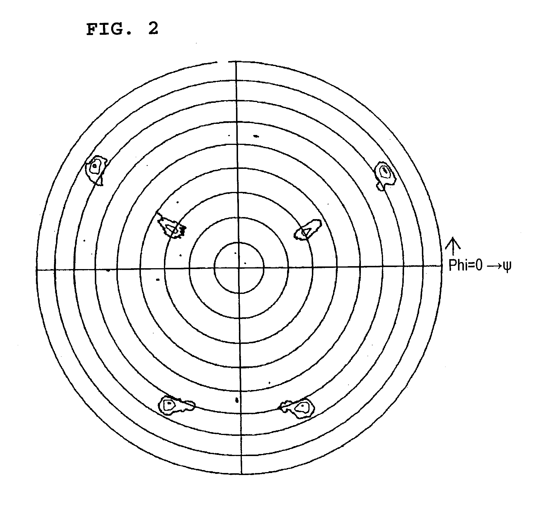
[0080] FIG. 4 shows an X-ray diffraction pole figure obtained in this second example in which X-rays were incident on the (200) plane of the Al electrode layer 4. As shown in FIGS. 5 and 6, additional lines were drawn for illustrating the diffraction pattern shown in FIG. 4.

[0081] As shown in FIGS. 4, 5, and 6, the Al electrode layer 4 was a thin epitaxial film in which diffraction spots having a plurality of symmetry centers were observed. Twelve spots in FIGS. 4, 5 and 6 show the detection of reflection signals from the (200) plane of the Al.

[0082] As can be apparently seen in FIG. 5, the twelve diffraction spots thus detected were two sets of six-fold symmetry spots. As in the first example, the ...

third example

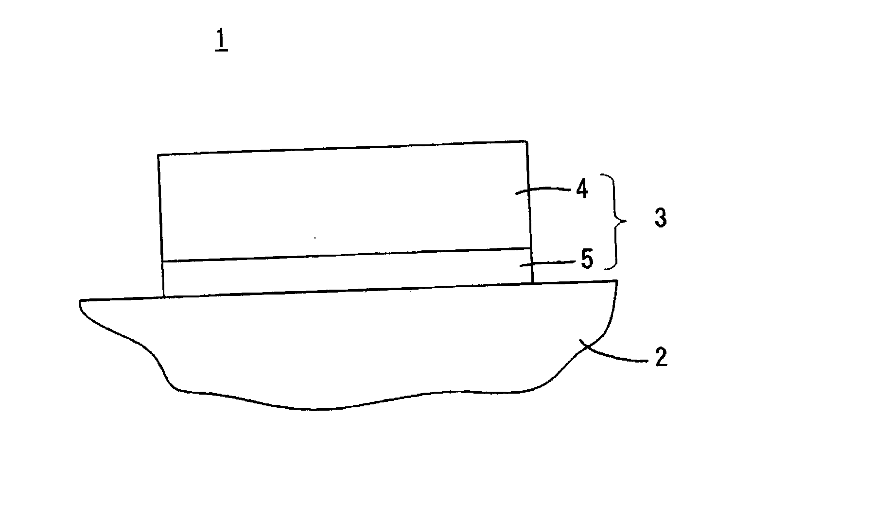
[0088] In a third example, a surface acoustic wave filter was formed having the structure shown in FIG. 1 as the surface acoustic wave device 1.

[0089] First, a piezoelectric substrate 2 composed of a 36.degree. Y-cut LiTaO.sub.3 single crystal was prepared.

[0090] Subsequently, on the piezoelectric substrate 2, the underlying electrode layer 5 was formed by an electron beam deposition method using Ti at a temperature of about 70.degree. C. so as to have a thickness of about 20 nm, and was then cooled to a temperature of about 50.degree. C. or less in an evacuated state.

[0091] After the cooling described above, the Al electrode layer 4 was formed using Al so as to have a thickness of about 100 nm.

[0092] The Al electrode layer 4 thus formed had a half value width of the Al (111) of approximately 2.degree. measured by X-ray diffraction. As a comparative example, when the underlying electrode layer 5 and the Al electrode layer 4 were formed without heating as described above, the half va...

fourth example

[0095] In a fourth example, a surface acoustic wave filter was formed as a surface acoustic wave device 1a having the structure shown in FIG. 8.

[0096] First, a piezoelectric substrate 2 composed of a 36.degree. Y-cut LiTaO.sub.3 single crystal was prepared.

[0097] Subsequently, on the piezoelectric substrate 2, the underlying electrode layer 5 was formed by an electron beam deposition method using Ti at a temperature of about 70.degree. C. so as to have a thickness of about 10 nm, and was then cooled to a temperature of about 50.degree. C. or less in an evacuated state.

[0098] After the cooling described above, an intermediate electrode layer 6 composed of Ti, which was the same material as that for the underlying electrode layer 5, was formed at a temperature of about 50.degree. or less so as to have a thickness of about 10 nm.

[0099] The Al electrode layer 4 was then formed using Al so as to have a thickness of about 100 nm.

[0100] The Al electrode layer 4 thus formed had a half value...


PUM

PropertyMeasurementUnit
temperatureaaaaaaaaaa

Abstract

A surface acoustic wave device has superior electrical power resistance that is obtained by improving stress migration resistance of electrodes. In order to form at least one electrode, for example, on a theta rotation Y-cut (theta=36° to 42°) LiTaO3 piezoelectric substrate, an underlying electrode layer including Ti or Cr as a primary component is formed, and an Al electrode layer including Al as a primary component is then formed on this underlying electrode layer. The Al electrode layer is an oriented film grown by epitaxial growth and is also a polycrystalline thin film having a twin structure in which a diffraction pattern observed in an X-ray diffraction pole figure has a plurality of symmetry centers.

Description

[0001] 1. Field of the Invention[0002] The present invention relates to surface acoustic wave devices, such as surface acoustic wave resonators or surface acoustic wave filters, and manufacturing methods therefor, and more particularly, relates to an electrode structure of a surface acoustic wave device and a forming method therefor.[0003] 2. Description of the Related Art[0004] As has been well known, surface acoustic wave devices are electronic elements including a surface acoustic wave in which mechanical vibration energy is concentrated only in the vicinity of surfaces of a solid material and is then propagated. In addition, the surface acoustic wave devices are each generally composed of a piezoelectric substrate having piezoelectric properties and electrodes, such as interdigital electrodes and / or grating electrodes, disposed on the piezoelectric substrate for processing electrical signals and surface acoustic waves.[0005] In the surface acoustic wave devices described above, ...

Claims


Application Information

Patent Timeline
Patent Type & Authority Applications(United States)
IPC IPC(8): H03H9/02
CPCH03H9/02929Y10T29/42Y10T29/49128Y10T29/49155Y10T29/49135Y10T29/49126Y10T29/4913H03H3/08
Inventor NAKAGAWARA, OSAMUSAEKI, MASAHIKOINOUE, KAZUHIRO
Owner MURATA MFG CO LTD
Why Eureka
Try Eureka