Method of forming a planar polymer transistor using substrate bonding techniques

a polymer transistor and substrate technology, applied in the direction of thermoelectric device junction materials, semiconductor devices, electrical equipment, etc., can solve the problems of inability to meet the requirements of use, the most sensitive portion of the body element is exposed to process-induced contamination, and the device has poor performance and inconsistent properties

Inactive Publication Date: 2003-07-17
IBM CORP
View PDF0 Cites 41 Cited by
  • Summary
  • Abstract
  • Description
  • Claims
  • Application Information

AI Technical Summary

Problems solved by technology

However, despite considerable research and development effort, organic-based TFTs have not yet reached commercialization, at least, in part, due to relatively poor device characteristics of prior art organic TFTs.
Problems with bottom-contact devices are well-known to those skilled in the art.
However, topography of the bottom source and drain contacts in the prior art causes problems with printing the organic semiconductor, which would be remedied by using a planar substrate.
First, the corner thinning problem due to topography, and second, the most sensitive portion of the body element is exposed to process-induced contamination.
The resulting devices have poor performance and inconsistent properties.
The body surface, especially in the channel region, deteriorates due to the unwanted chemical reaction.
In both of the bottom-contact devices described above, there is a well-documented problem with ensuring good contact between the electrodes and the organic semiconductor.
However, the topography of the bottom electrodes may still hamper film formation and reduce the contact area.

Method used


Image

  • Method of forming a planar polymer transistor using substrate bonding techniques
  • Method of forming a planar polymer transistor using substrate bonding techniques
  • Method of forming a planar polymer transistor using substrate bonding techniques

Examples


Embodiment Construction

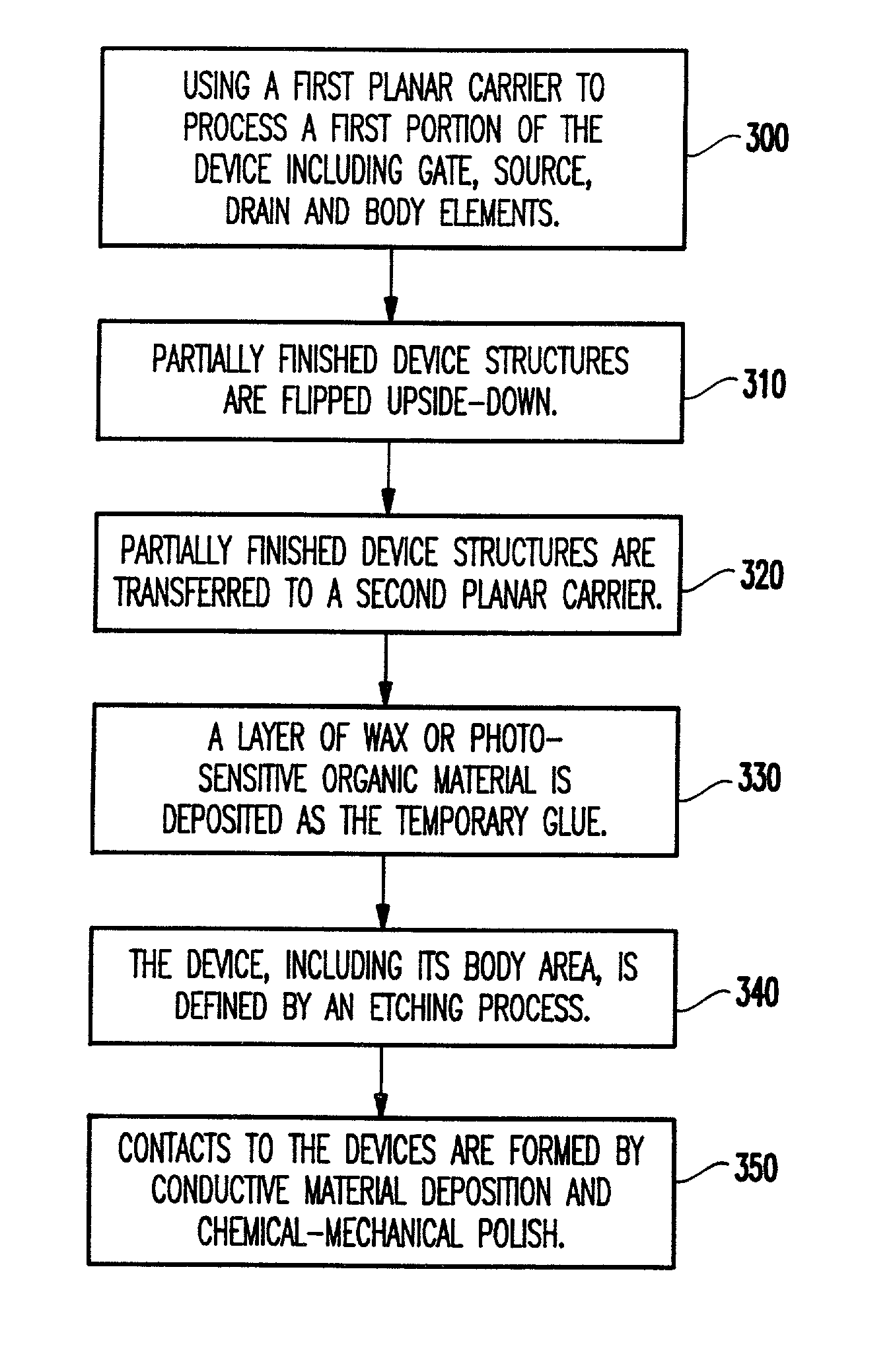
[0035] As mentioned above, there is a need for an improved structure and method for producing a planar polymer transistor which does not have the problems inherent with the prior art devices, such as the corner thinning problem due to topography, and having the most sensitive portion of the body element exposed to process-induced contamination. According to the present invention, a new and improved structure of a thin-film transistor is disclosed, as well as a method for producing the same.

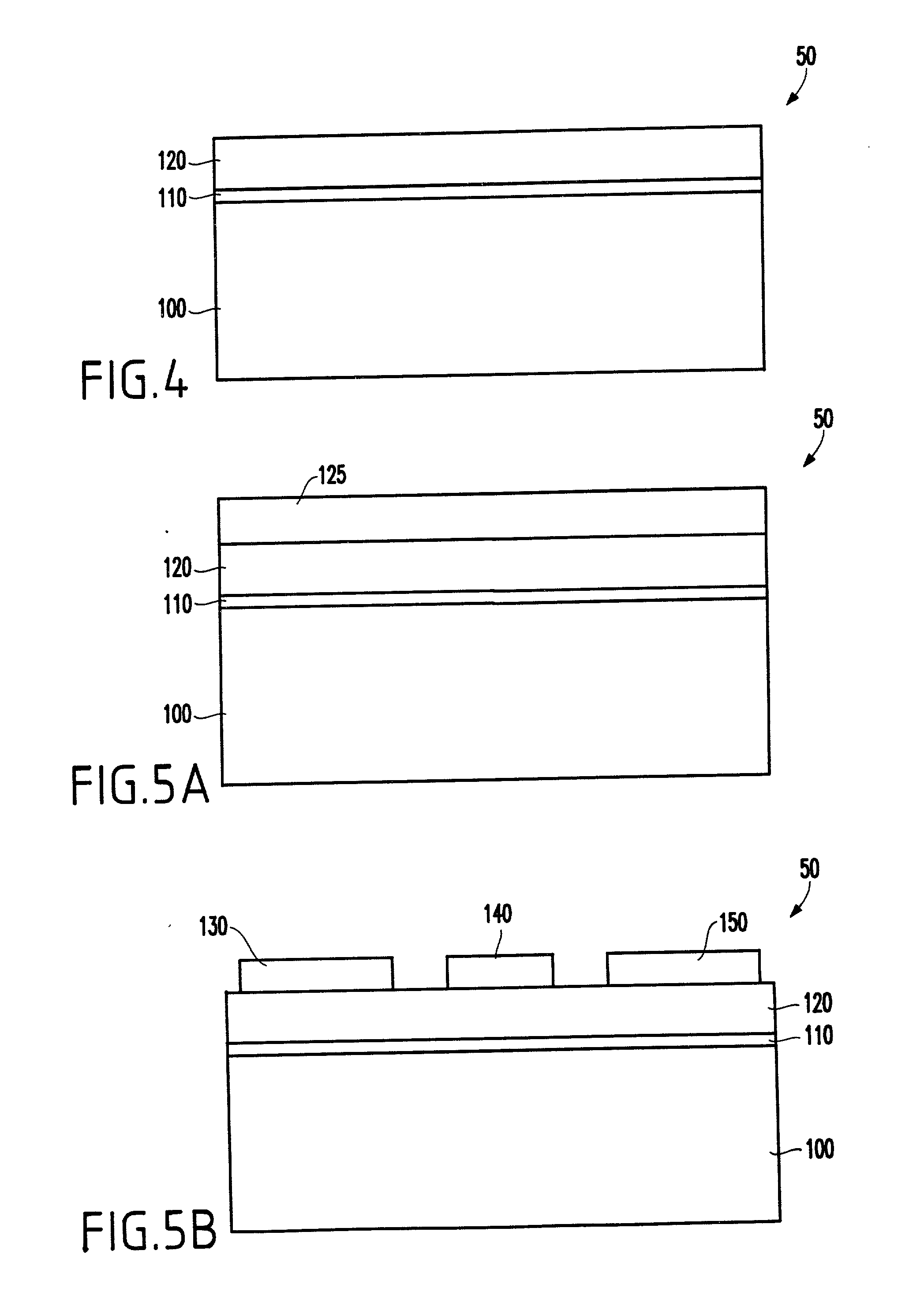
[0036] Referring now to the drawings, and more particularly to FIGS. 4 through 11, there are shown preferred embodiments of the method and structures according to the present invention. Specifically, FIG. 4 shows a partially completed thin-film transistor device 50 comprising an insulating polymer 120 coated on top of a thin layer of wax 110 formed on a substrate carrier 100. The thin layer of wax 110 allows for the ease of material transference at a later stage. The substrate 100 can be glass, ce...


PUM


Abstract

A structure and method of forming a fully planarized polymer thin-film transistor by using a first planar carrier to process a first portion of the device including gate, source, drain and body elements. Preferably, the thin-film transistor is made with all organic materials. The gate dielectric can be a high-k polymer to boost the device performance. Then, the partially-finished device structures are flipped upside-down and transferred to a second planar carrier. A layer of wax or photo-sensitive organic material is then applied, and can be used as the temporary glue. The device, including its body area, is then defined by an etching process. Contacts to the devices are formed by conductive material deposition and chemical-mechanical polish.

Description

[0001] 1. Field of the Invention[0002] The present invention generally relates to semiconductor technology and device designs, and more particularly to an organic-based thin-film transistor device and a method for producing the same.[0003] 2. Description of the Related Art[0004] Thin-film transistors (TFTs) with active organic layers and polymer-based electronic components are emerging as an inexpensive alternative to silicon-based TFTs for some applications. The use of organic and polymeric materials provides two main advantages: First, organic-based devices can be produced using a simpler and less expensive fabrication process in contrast to the expensive equipment and processing associated with silicon processing. Second, it is possible to fabricate the devices on flexible plastic substrates due to the ability to process organic materials at lower temperatures, and due to the greater mechanical flexibility of organic-based components relative to inorganic materials such as silico...

Claims


Application Information

Patent Timeline
Patent Type & Authority Applications(United States)
IPC IPC(8): H01L21/00H01L21/336H01L29/786H01L51/05H01L35/24H01L51/00H01L51/40
CPCH01L51/0001H01L51/0024H01L51/0545H01L51/0541H01L51/0516H10K71/00H10K71/50H10K10/468H10K10/466H10K10/464
Inventor BREEN, TRICIA L.CLEVENGER, LAWRENCE A.HSU, LOUIS L.WANG, LI-KONGWONG, KWONG HON
Owner IBM CORP
Why Eureka
Try Eureka