Supercharge Your Innovation With Domain-Expert AI Agents!

Sacrificial seed layer process for forming c4 solder bumps

a seed layer and c4 technology, applied in the direction of soldering apparatus, semiconductor/solid-state device details, manufacturing tools, etc., can solve the problems of high-lead solder bumps that melt at temperatures greater than 300.degree. c., cannot be universally applicable, and structure does not necessarily produce a reliable structur

Inactive Publication Date: 2003-08-21
GLOBALFOUNDRIES US INC
View PDF0 Cites 41 Cited by
  • Summary
  • Abstract
  • Description
  • Claims
  • Application Information

AI Technical Summary

Problems solved by technology

However, there are more recent applications in which it can actually be detrimental to include copper as a BLM constituent of the seed layer.
Many semiconductor packages now utilize organic carriers, which cannot tolerate temperatures in excess of 240.degree. C.
In addition, many high performance semiconductor devices are now being designed with low K dielectric materials that become unstable at temperatures above 300.degree. C.
For these reasons, high-lead solder bumps that melt at temperatures greater than 300.degree. C. are not universally applicable.
Unfortunately, the presence of copper in the final BLM structure does not necessarily produce a reliable structure.
Upon heat treatment, copper reacts so aggressively in the presence of Sn-rich solder bumps that a BLM structure containing copper becomes unstable and deteriorates rapidly.
This solution does minimize exposure to BLM attack, but under extreme field conditions, the high-Sn solder has the potential to eventually attack the copper portion of the BLM from the periphery of the C4 solder balls.
Completely removing copper from the seed layer is plausible, but renders it extremely difficult to electroplate C4 solder balls uniformly without a sufficiently conductive seed layer.
Changing plating baths adds complexity and an additional step in the bump plating process and requires intermediate steps of plating the barrier layer onto the workpiece for a timed interval, removal of the workpiece from the barrier layer bath, rinsing the workpiece and reinsertion of the workpiece into a C4 solder bump plating bath.
A problem with this procedure is that the titanium is a poor conductor and for a large device the current / resistance (IR) voltage drop will result in excessive variations in the thickness of the solder balls plated in the electroplating bath.
The fact that the photoresist is absent results in a different geometry of C4 solder bump in the form of a mushroom with the disadvantage that mushrooms can cause formation of short circuits on reflow (melting).
Also, mushrooming makes it difficult to control dimensional and compositional uniformity.

Method used


Image

  • Sacrificial seed layer process for forming c4 solder bumps
  • Sacrificial seed layer process for forming c4 solder bumps
  • Sacrificial seed layer process for forming c4 solder bumps

Examples


second preferred embodiment

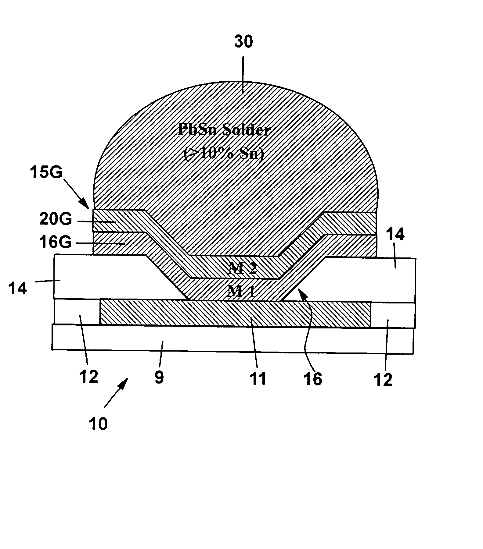
[0058] A second embodiment of this invention is implemented by modification of the process of FIGS. 3A-3B by adding a barrier layer or layers between the intermediate M2 layer 20 and the C4 solder bump 26 as illustrated by FIGS. 4A-4H. For example, a barrier layer 28 composed of nickel (Ni) can be electroplated in the through holes 23' as shown in FIG. 4C onto the top surface of intermediate M2 layer 20 into the windows 23 in the photoresist mask PR' in the shape of the through holes 23' at the bottom of the windows 23 (as a base for electroplating of C4 solder bumps 26) after removal of the copper of CM layer 22, but prior to the deposition of the C4 solder bumps 26, as outlined in the following process sequence: P0 1. Referring to FIG. 4A, deposit a multi-layer seed layer stack 15 as in FIG. 3A, which includes the M1 adhesion layer 16, the intermediate, metallic, M2 layer 20 and the metallic surface, CM layer 22 formed above M2 layer 20, deposited in that order on the contact 11 a...


PUM

PropertyMeasurementUnit
Adhesion strengthaaaaaaaaaa
Electrical conductoraaaaaaaaaa

Abstract

Start with a semiconductor substrate with contacts exposed through an insulating layer. Form a base over the contacts, with the base composed of at least one metal layer. Then form a conductive metal layer over the base. Form a mask over the top surface of the conductive metal layer with C4 solder bump openings therethrough with the shape of C4 solder bump images down to the surface of the conductive metal layer above the contacts. Etch away the exposed portions of the conductive metal layer below the C4 solder bump openings to form through holes in the conductive metal layer exposing C4 solder bump plating sites on the top surface of the base below the C4 solder bump openings with the conductive metal layer remaining intact on the periphery of the through holes at the C4 solder bump plating sites. As an option, form a barrier layer over the plating sites next. Form C4 solder bumps on the plating sites on the base / barrier layer within the C4 solder bump openings, with the C4 solder bumps being in contact with the conductive metal layer on the periphery of the through holes. Remove the mask. Etch away the remainder of the conductive metal layer, and etch away the base aside from the C4 solder bumps forming BLM pads. Then reflow the C4 solder bumps to form C4 solder balls.

Description

[0001] 1. Field of the Invention[0002] This invention relates to processes for forming C4 solder bumps and more particularly to the metallurgy employed for enhanced characteristics of the joints.[0003] 2. Description of Related Art[0004] Controlled Collapse Chip Connection (C4) solder ball, flip chip connections have been used for more than thirty years to provide flip chip interconnections between semiconductor devices and substrates. Cylindrical C4 solder bumps are formed above an insulation layer and above the exposed surfaces of connector pads each of which is exposed through a VIA hole in the insulation layers. Later the C4 solder bumps are heated above the melting point until the C4 solder bumps reflow by controlled collapse to form C4 solder balls. The actual C4 solder bumps may be fabricated using a number of different processing techniques, including evaporation, screening, and electroplating. Fabrication by electroplating requires a series of basic steps which typically in...

Claims


Application Information

Patent Timeline
IPC IPC(8): B23K35/00H01L21/288H01L21/60H01L23/485
CPCB23K35/001B23K35/007H01L2924/01033H01L2924/01024H01L2924/01019H01L2924/014H01L2924/01327H01L21/2885H01L24/03H01L24/05H01L24/11H01L2224/03912H01L2224/03914H01L2224/0401H01L2224/05599H01L2224/1147H01L2224/11472H01L2224/13023H01L2224/13099H01L2224/131H01L2924/01002H01L2924/01006H01L2924/01013H01L2924/01014H01L2924/01015H01L2924/01022H01L2924/01027H01L2924/01028H01L2924/01029H01L2924/01047H01L2924/0105H01L2924/01059H01L2924/01074H01L2924/01077H01L2924/01078H01L2924/01079H01L2924/01082H01L2924/01322H01L2924/00014
Inventor FANTI, LISA A.KNARR, RANDOLPH F.ROGGEMAN, ERIK J.SRIVASTAVA, KAMALESH K.
Owner GLOBALFOUNDRIES US INC
Features
  • R&D
  • Intellectual Property
  • Life Sciences
  • Materials
  • Tech Scout
  • Unparalleled Data Quality
  • Higher Quality Content
  • 60% Fewer Hallucinations
Learn More