Mask read only memory device and fabrication method thereof

Inactive Publication Date: 2003-11-06
MACRONIX INT CO LTD
View PDF13 Cites 2 Cited by
  • Summary
  • Abstract
  • Description
  • Claims
  • Application Information

AI Technical Summary

Benefits of technology

0020] According to the mask ROM device and the fabrication thereof of the present invention, the problem of misalignment in code implantation as in the prior art is prevented.
0021] Further, the mask ROM device and the fabrication thereof of the present invention can prevent an increase of the device's resistance.
0022] Since the redundancy cells of the mask ROM device of the present invention are

Problems solved by technology

However, if a misalignment occurs between the coding mask and the memory device, the reliability of the device is adversely affected.
Moreover, the high-energy, high dosage coding implantation process would increase the resistance of the entire memory device, affecting the characteristics of the device.
Further, as the device dimensions is being scaled down, any micro defects or damages on the memory

Method used


Image

  • Mask read only memory device and fabrication method thereof
  • Mask read only memory device and fabrication method thereof
  • Mask read only memory device and fabrication method thereof

Examples


Embodiment Construction

[0030] FIGS. 2A-2E are schematic, cross-sectional views illustrating the process flow of a manufacturing method for a mask ROM device according to one preferred embodiment of the present invention.

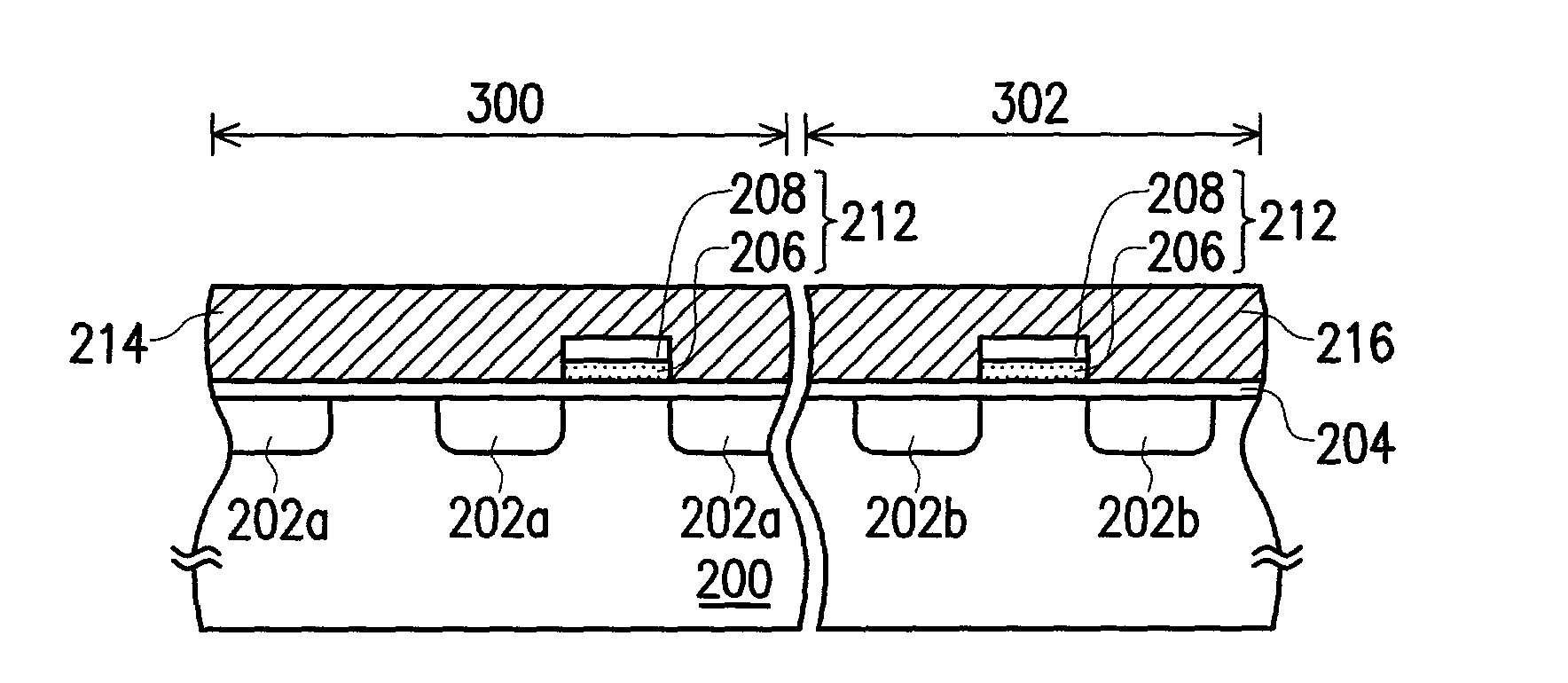
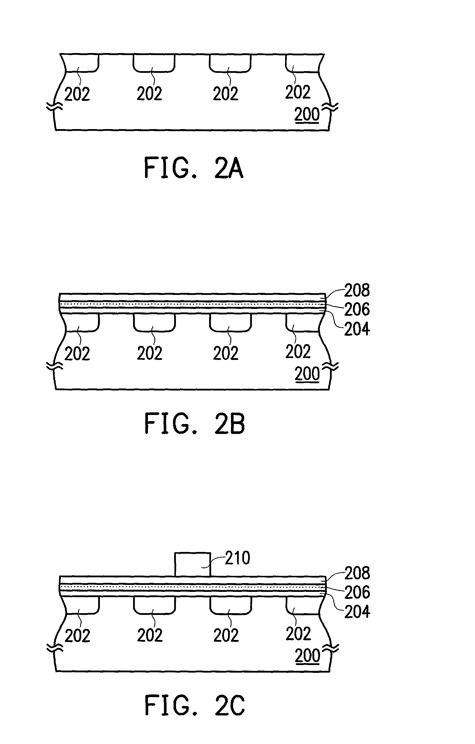
[0031] Referring to FIG. 2A, a buried drain region 202 is formed in a substrate 200 as a bit line. Forming the buried drain region 202 includes forming a patterned photoresist layer (not shown in Figure) on the substrate 200, followed by performing an ion implantation process.

[0032] Referring to FIG. 2B, a gate oxide layer 204 is formed on the surface of the substrate 200, wherein the gate oxide layer 204 is about 20 angstroms to about 30 angstroms thick. A silicon nitride layer 206 and a silicon oxide layer 208 are further sequentially formed on the gate oxide layer 204. The silicon nitride layer 206 is about 50 angstroms to 70 angstroms thick, while the silicon oxide layer 208 is about 90 angstroms to about 130 angstroms thick.

[0033] Continuing to FIGS. 2C and 2D, a patterned photoresist...


PUM


Abstract

A mask ROM and a fabrication method thereof are described. The method includes forming a buried drain region in the substrate and forming a gate oxide layer on the substrate. A patterned dual-layer structure dielectric layer is formed on the gate oxide layer. A conductive layer, which is perpendicular to the direction of the buried drain region, is then formed on the gate oxide layer and on the dual-layer structure dielectric layer to form a plurality of code memory cells. The code memory cells that comprise the dual-layer structure dielectric layer correspond to the logic state of "0", while the memory cells that do not comprise the dual-layer structure dielectric layer correspond to the logic state of "1".

Description

CROSS-REFERENCE TO RELATED APPLICATION[0001] This application claims the priority benefit of Taiwan application serial no. 91109316, filed May 6, 2002.BACKGROUND OF THE INVENTION[0002] 1. Field of the Invention[0003] The present invention relates to a memory device and a fabrication method thereof. More particularly, the present invention relates to a mask read only memory (ROM) device and a fabrication method thereof.[0004] 2. Background of the Invention[0005] Mask ROM device is a very fundamental type of read-only memory devices, in which a photomask layer is used to define a connection between a metal line and a memory cell or an ion implantation process is used to adjust the threshold voltage to achieve the "on" and "off" of the memory cell. When there are changes in the products of a mask ROM device, no dramatic modification is demanded by the manufacturing process. Only one set of photomask has to be replaced. Therefore, the manufacturing of a mask ROM device is appropriate fo...

Claims


Application Information

Patent Timeline
IPC IPC(8): H01L21/8246H01L27/112
CPCH01L27/11233H01L27/112H10B20/00H10B20/36
Inventor CHANG, YAO-WENLU, TAO-CHENG
Owner MACRONIX INT CO LTD
Why Eureka
Try Eureka