

Conductive layer pattern and method for forming the same, wiring board, electronic device, electronic appliances and noncontact card medium
a technology of conductive layer and pattern, which is applied in the direction of conductive layer on insulating support, resistive material coating, cable/conductor manufacturing, etc., can solve the problems of poor productivity, large facilities such as vacuum apparatus and complicated process, and high production cos
- Summary
- Abstract
- Description
- Claims
- Application Information
AI Technical Summary
Benefits of technology
Problems solved by technology
Method used
Image

Examples
example 2
[0133] Into a dispersion of gold fine particles (a liquid prepared by diluting "perfect gold (trade name)" made by Vacuum Metallurgical Co. with toluene to a viscosity of 3 mPa.multidot.s) used in Example 1, 10% by weight of chlorotrimethyl phosphine gold (I) as an organometallic compound was added and dissolved. A conductive pattern was prepared by the same process as in Example 1, except that the fluid obtained as described above was used.
[0134] Since chlorotrimethyl phosphine gold (I) is dissolved in toluene, it is readily absorbed into the receiving layer together with toluene as a solvent, it is decomposed by baking at 300.degree. C. to precipitate gold. Consequently, the receiving layer under the position where droplets are disposed was converted into a conductive part. This part had a lower resistance than the part prepared by allowing only the conductive particles to permeate in Example 1.
example 3
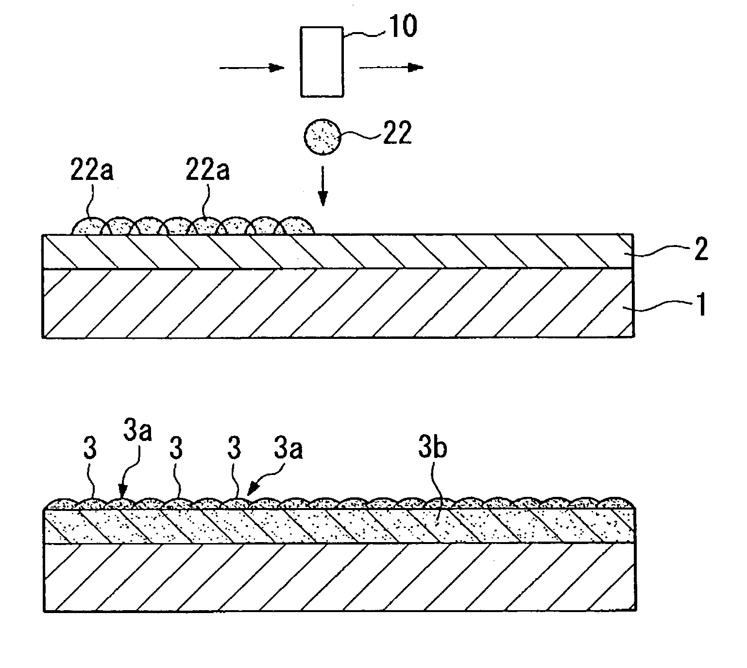
[0135] After discharging a fluid onto the substrate from the droplet discharge head by the same method as in Example 1, the substrate was heat treated at a temperature of 100.degree. C. in place of heating at 300.degree. C. for 30 minutes. This treatment was applied for removing the dispersing medium in the droplets, and the conductive fine particles are not bonded (sintered) with each other at this temperature.
[0136] The droplets were discharged again by the same method as in Example 1 for repeated application on the lines comprising the conductive fine particles obtained by the heat treatment. Then, since the layer (aggregates) comprising the conductive fine particles that has been formed serves as a receiving layer, the thickness of the layer was doubled (10 .mu.m) with the same pattern.
[0137] The particles were applied several times and the layer formed was finally baked (sintered), and a conductive layer pattern having a thickness approximately proportional to the repeated numb...
example 4
[0138] A multilayer wiring board was prepared by the method for forming the conductive pattern in Examples 1 and 3.
[0139] A post pattern was formed so as to be continuous to a part of the line that had been formed as a repeatedly applied pattern in Example 3. Then, the pattern was baked at a high temperature to form the conductive pattern and a post connected thereto.
[0140] Subsequently, polyimide was applied so as to cover the receiving layer and the conductive pattern thereon while allowing the surface of the post to be exposed. An inter-insulation layer was formed by curing the polyimide layer. Polyimide was applied using a solution of a polyimide precursor and the same droplet discharge apparatus as used for discharging the solution containing the conductive fine particles. The pattern was applied so as to detour around the post.
[0141] A receiving layer was formed again in the inter-insulation layer by the same method as in Example 1, and a second conductive pattern was formed t...
PUM
| Property | Measurement | Unit |
|---|---|---|
| thickness | aaaaa | aaaaa |
| void diameter | aaaaa | aaaaa |
| mean particle diameter | aaaaa | aaaaa |
Abstract
Description
Claims
Application Information