Miniature RF and microwave components and methods for fabricating such components

a technology of microwave components and components, applied in the direction of waveguides, non-resonant long antennas, instruments, etc., can solve the problems of affecting the performance of the microwav

Active Publication Date: 2003-12-04
MEMGEN
View PDF70 Cites 134 Cited by
  • Summary
  • Abstract
  • Description
  • Claims
  • Application Information

AI Technical Summary

Benefits of technology

0039] It is an aspect of the invention to provide a microminiature RF or microwave coaxial component, that includes an inner conductor that has an axis which is substantially coaxial with an axis an outer conductor wherein the inner and outer conductors are spaced from one another by a dielectric gap wherein a minimum cross-sectional dimension from an inside wall of the outer conductor to an opposing inside wall of the outer conductor is less than about 200 .mu.m. In a specific variation of this aspect of the invention the outer conductor has a substantially rectangular cross-sectional configuration.

Problems solved by technology

The CC mask plating process is distinct from a "through-mask" plating process in that in a through mask plating process the separation of the masking material from the substrate would occur destructively.
Fundamental electromagnetic theory shows that rectangular coax can provide very similar performance to circular coax, although analytic methods of design are lacking.
There is an entire family of passive microwave functions that can not be realized in semiconductor ICs, or that can be realized only with a significant penalty in performance.
An example of a function with inferior IC performance is frequency multiplexing--i.e., the routing of microwave power from one input port into a number of different output ports depending on frequency.
Such integration addresses a growing problem in the IC industry which is the interconnecting and routing of high-frequency analog and digital signals within chips.
Transmission of very sharp edges down conventional (stripline) transmission lines on Si invariably distorts, or spreads out, the edge because of dispersion and losses on the line.
However, as three materials may or may not be deposited on each layer, this process adds not only complexity of the process but also can yield structures of enhanced functionality and versatility.
Though this question was asked previously, the answer may have changed due to a different pattern of conductive material to be deposited or due to the removal of a previously supplied seed layer because it is incompatible with the second conductive material that is to be deposited.
This independence of the electrode size and contact gaps is not possible if both must lie on a planar substrate.
It is believed that such a configuration will result in reduced ohmic resistance has a desired current travels around the inductive path.
On the other hand as the coupling between the two inductors is probably reduced, there is probably an associated loss of net inductance.

Method used


Image

  • Miniature RF and microwave components and methods for fabricating such components
  • Miniature RF and microwave components and methods for fabricating such components
  • Miniature RF and microwave components and methods for fabricating such components

Examples


Embodiment Construction

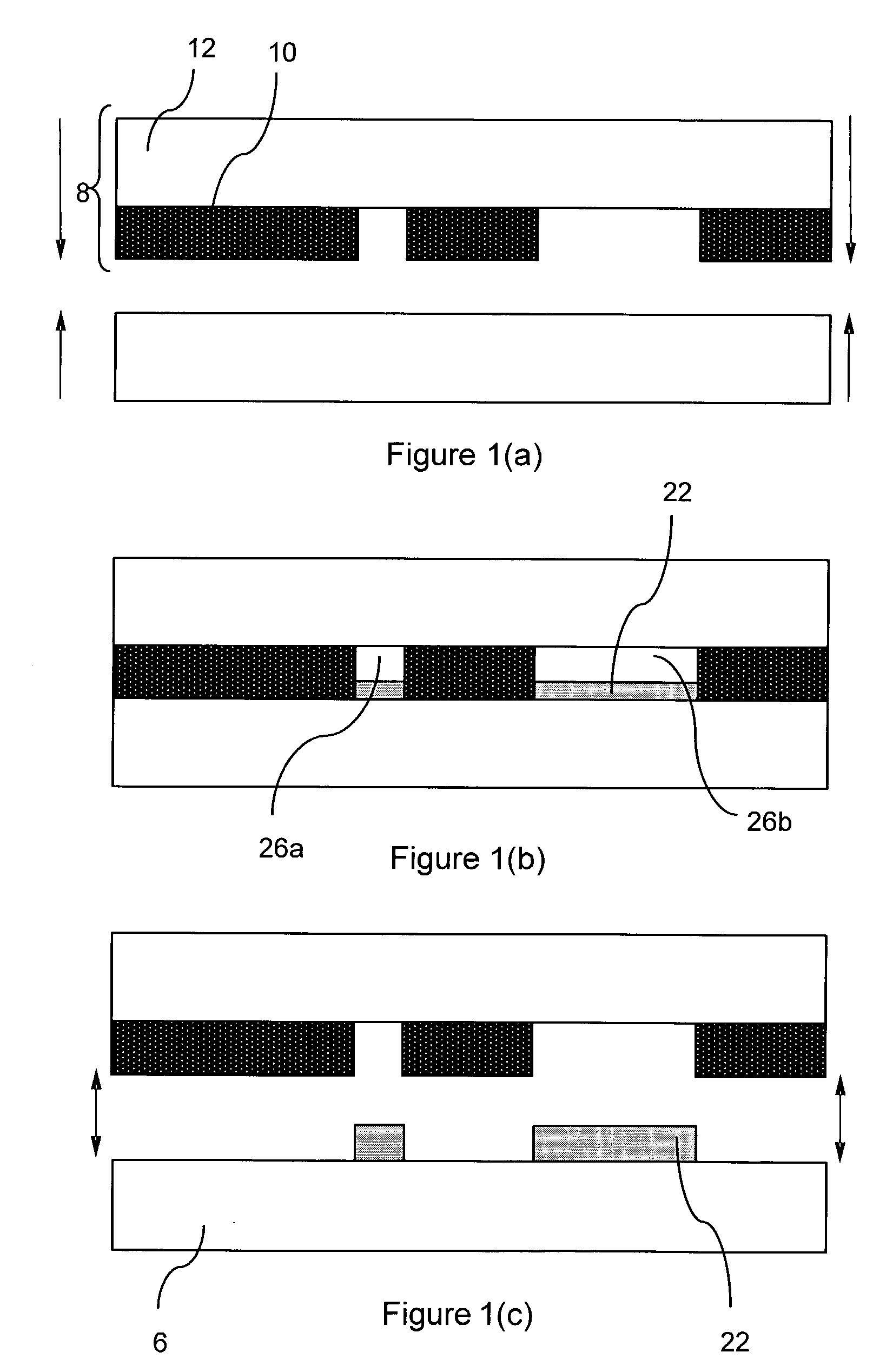
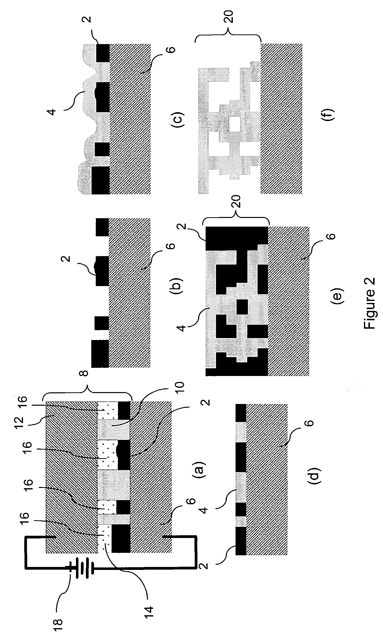
[0102] A basic process of electrochemically forming layers of multilayer three-dimensional structures was presented in FIGS. 1(a)-1(c), while FIGS. 2(a)-2(f) applied the layer forming technique to a plurality of overlaid layers (i.e. face-to-face contacting of layers regardless of whether successive layers are formed above, below, or beside previously formed layers). Various possible apparatus components were discussed with the aid of FIGS. 3(a)-3(c). This apparatus and these processes may be used in forming structures according to some embodiments of the invention. Other apparatus and processes may also be used.

[0103] For example, in some embodiments process variations may be used to yield cavities within the conductive structures that are filled completely or partially with a dielectric material, a conductive material embedded in a dielectric, or a magnetic material (e.g. a powdered ferrite material embedded in a dielectric binder or sintered after placement). The dielectric mater...


PUM

PropertyMeasurementUnit
frequencyaaaaaaaaaa
frequencyaaaaaaaaaa
frequencyaaaaaaaaaa

Abstract

RF and microwave radiation directing or controlling components are provided that may be monolithic, that may be formed from a plurality of electrodeposition operations and/or from a plurality of deposited layers of material, that may include switches, inductors, antennae, transmission lines, filters, and/or other active or passive components. Components may include non-radiation-entry and non-radiation-exit channels that are useful in separating sacrificial materials from structural materials. Preferred formation processes use electrochemical fabrication techniques (e.g. including selective depositions, bulk depositions, etching operations and planarization operations) and post-deposition processes (e.g. selective etching operations and/or back filling operations).

Description

[0001] This application claims priority to U.S. Provisional Patent Application Nos.: 60 / 338,638 filed on Dec. 3, 2001; 60 / 340,372 filed on Dec. 6, 2001; 60 / 379,133 filed on May 7, 2002; 60 / 379,182 filed on May 7, 2002; 60 / 379,184 filed on May 7, 2002; 60 / 415,374 filed on Oct. 1, 2002; 60 / 379,130 filed on May 7, 2002 and 60 / 392,531 filed on Jun. 27, 2002, all of which are incorporated herein by reference as if set forth in full.[0002] Embodiments of this invention relate to the field of electrical devices and their manufacture while specific embodiments relate to RF and microwave devices and their manufacture. More particularly embodiments of this invention relate to miniature passive RF and microwave devices (e.g. filters, transmission lines, delay lines, and the like) which may be manufactured using, at least in part, a multi-layer electrodeposition technique known as Electrochemical Fabrication.[0003] A technique for forming three-dimensional structures / devices from a plurality of...

Claims


Application Information

Patent Timeline
Patent Type & Authority Applications(United States)
IPC IPC(8): B81B3/00G01P15/08G01P15/125H01P1/202H01P3/06H01P5/18H01P11/00H05K3/46
CPCB81B2201/042G01P15/0802G01P15/125H01P1/202H01P3/06H01P5/183Y10T29/49018H01P11/005H01P11/007H05K3/4647C25D1/003Y10T29/49016Y10T29/49002H01P11/00B33Y10/00
Inventor BROWN, ELLIOTT R.EVANS, JOHN D.BANG, CHRISTOPHER A.COHEN, ADAM L.LOCKARD, MICHAEL S.SMALLEY, DENNIS R.GROSSER, MORTON
Owner MEMGEN
Why Eureka
Try Eureka