Laser irradiation method and method of manufacturing a semiconductor device

a laser irradiation and semiconductor technology, applied in the direction of individual semiconductor device testing, semiconductor/solid-state device testing/measurement, instruments, etc., can solve the problems of poor substrate processing efficiency, inferior heat resistance of glass substrate, and inability to achieve the effect of reducing the number of laser irradiation beams

Inactive Publication Date: 2003-12-11
SEMICON ENERGY LAB CO LTD
View PDF83 Cites 73 Cited by
  • Summary
  • Abstract
  • Description
  • Claims
  • Application Information

AI Technical Summary

Problems solved by technology

A glass substrate is inferior in heat resistance and is easily subjected to thermal deformation.
As a result, the efficiency of substrate processing is poor and there is an important problem of how to impr

Method used


Image

  • Laser irradiation method and method of manufacturing a semiconductor device
  • Laser irradiation method and method of manufacturing a semiconductor device
  • Laser irradiation method and method of manufacturing a semiconductor device

Examples


embodiment 1

[0173] Embodiment 1

[0174] This embodiment describes optical systems of laser irradiation apparatus used in the present invention, and the positional relation between a slit and each of the optical systems.

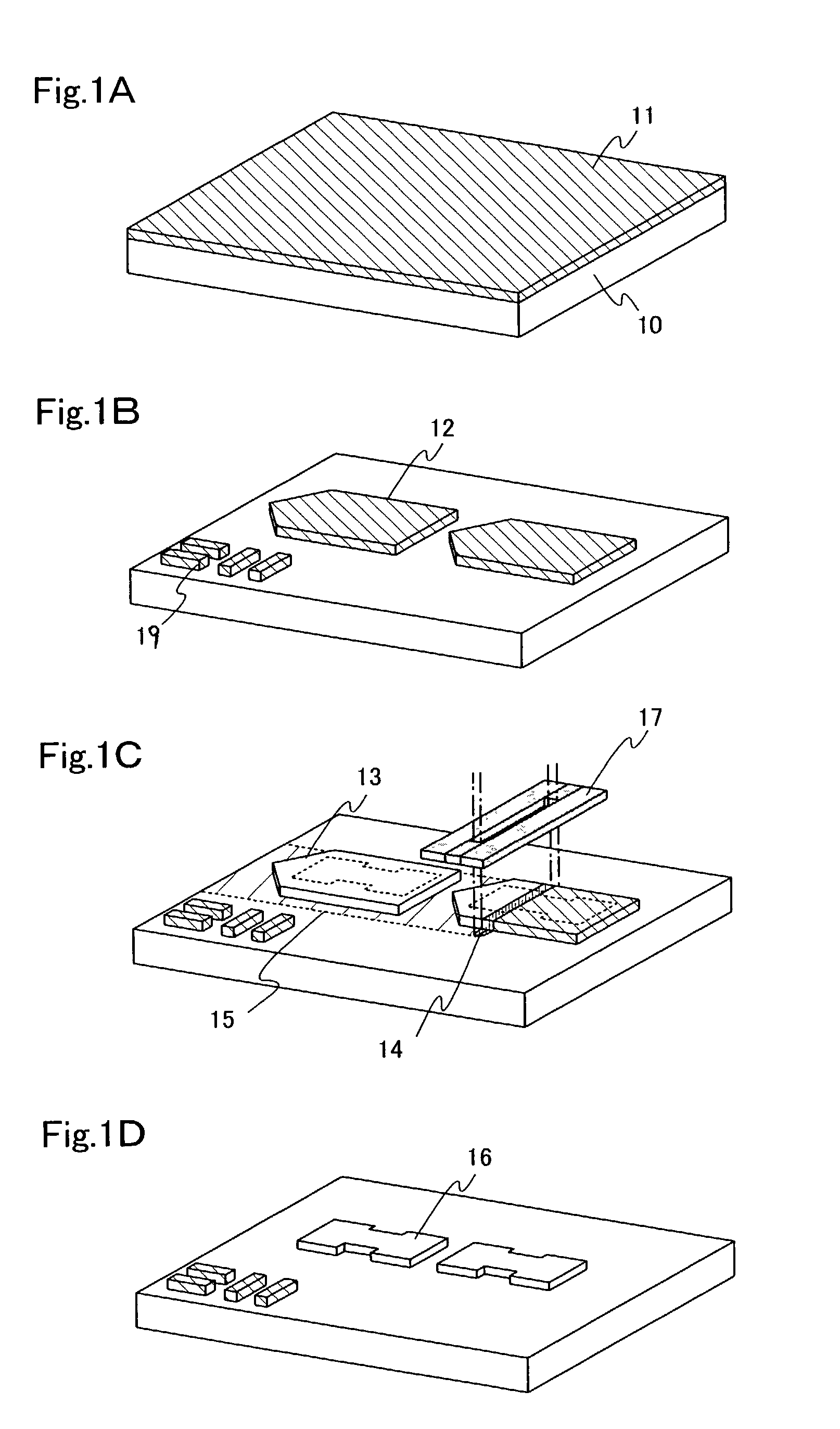
[0175] FIGS. 17A to 17D show optical systems of this embodiment. The optical system shown in FIG. 17A has two cylindrical lenses 401 and 402. Laser light entering from the direction indicated by the arrow passes through the two cylindrical lenses 401 and 402, which modify the shape of the beam spot of the laser light. The beam spot travels through a slit 404 to irradiate a processing object 403. Of the cylindrical lenses 401 and 402, 402 is closer to the processing object 403 and has a shorter focal length. In order to avoid return light and irradiate uniformly, the incident angle at which laser light enters the substrate is set to larger than 0.degree., desirably, 5 to 30.degree..

[0176] The optical system shown in FIG. 17B has a mirror 405 and a planoconvex spherical lens 406. Las...

embodiment 2

[0186] Embodiment 2

[0187] This embodiment describes an example in which plural laser oscillation apparatuses are used and the width of a beam spot of laser light is changed by an AO modulator in the middle of laser light irradiation.

[0188] In this embodiment, a computer grasps a laser light scanning path based on mask information inputted. Furthermore, this embodiment uses an AO modulator to change the direction of laser light outputted from any one of the plural laser oscillation apparatuses to prevent the redirected laser light from irradiating a processing object and thereby change the width of the beam spot in accordance with the mask shape. In this case, although the width of the beam spot is changed by the AO modulator, a region of the beam spot that is low in energy density still has to be blocked in the direction perpendicular to the scanning direction. Therefore, control of the slit width and blocking of laser light by the AO modulator have to be synchronized.

[0189] FIG. 18...

embodiment 3

[0208] Embodiment 3

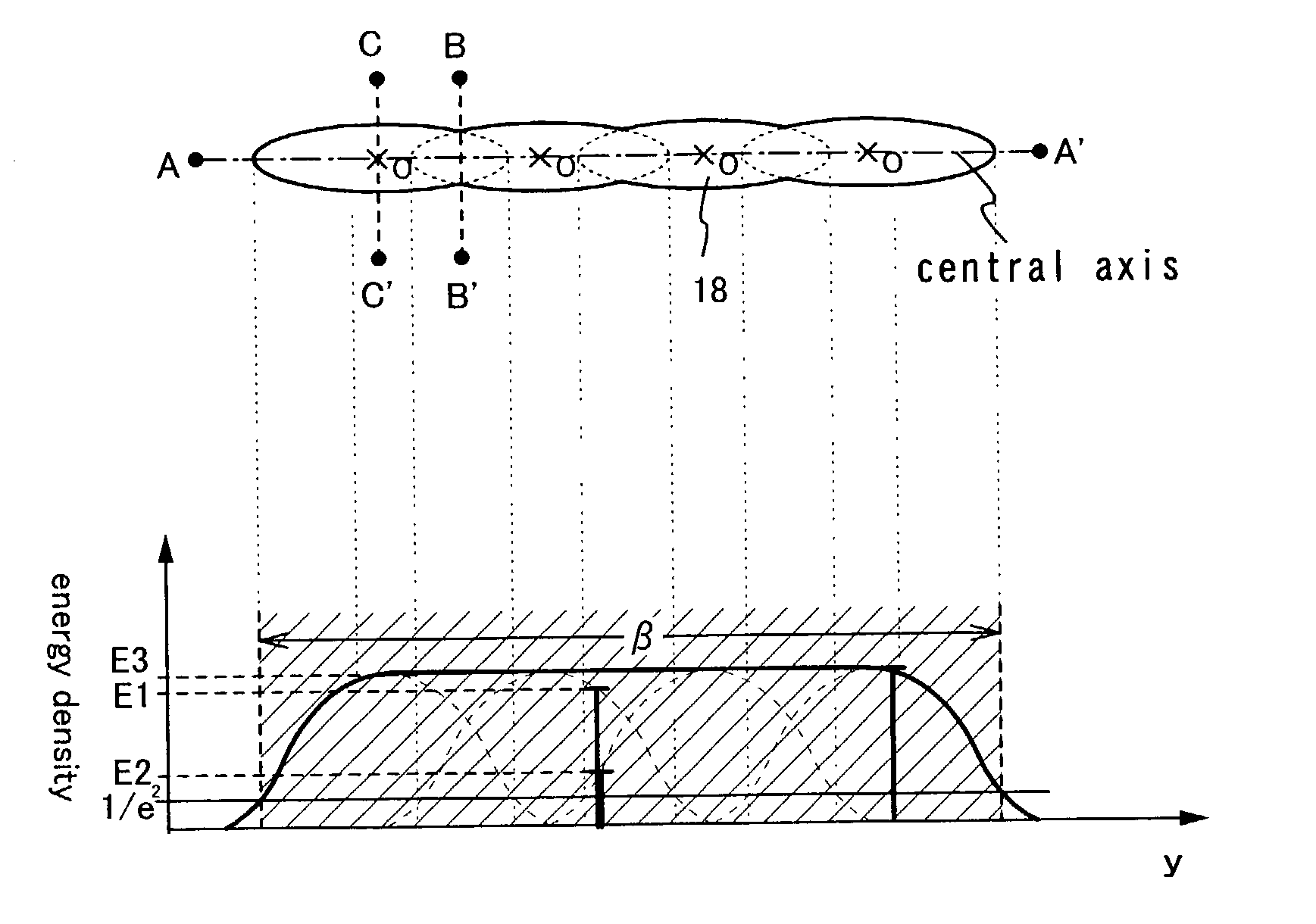
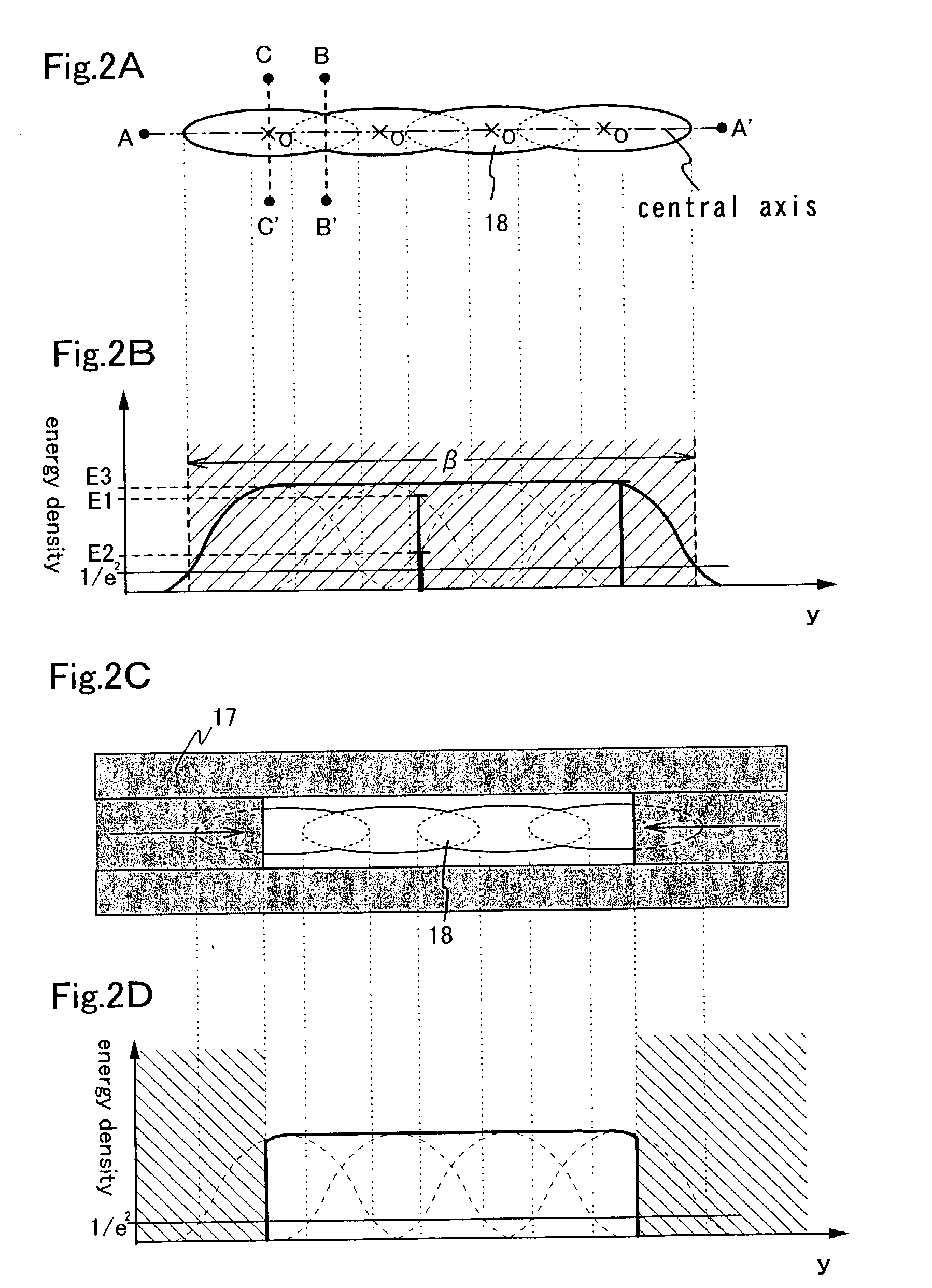
[0209] This embodiment describes, in relation to the energy density, the distance between centers of beam spots when they are overlapped.

[0210] In FIG. 21, the energy density distribution in the central axis direction of each beam spot is indicated by the solid line and the energy density distribution of the synthesized beam spot is indicated by the dashed line. The energy density value in the central axis direction of a beam spot generally follows Gaussian distribution.

[0211] Assume that, before synthesization, the distance in the central axis direction of a beam spot where the energy density is equal to or more than the peak value, 1 / e.sup.2, is 1. Then, the distance between peaks is given as X. An increase from the peak value of the average valley value to the peak value after synthesization is given as Y. The relation between X and Y obtained through simulation is shown in FIG. 38. Y in FIG. 38 is expressed as a percentage.

[0212] In FIG. 38, the energy differe...


PUM


Abstract

A method of manufacturing a semiconductor device is provided which uses a laser crystallization method capable of increasing substrate processing efficiency. An island-like semiconductor film including one or more islands is formed by patterning (sub-island). The sub-island is then irradiated with laser light to improve its crystallinity, and thereafter patterned to form an island. From pattern information of a sub-island, a laser light scanning path on a substrate is determined such that at least the sub-island is irradiated with laser light. In other words, the present invention runs laser light so as to obtain at least the minimum degree of crystallization of a portion that has to be crystallized, instead of irradiating the entire substrate with laser light.

Description

[0001] 1. Field of the Invention[0002] The present invention relates to a laser irradiation method for crystallizing a semiconductor film using a laser light or for performing activation after ion implantation and to a method of manufacturing a semiconductor device.[0003] 2. Description of the Related Art[0004] In recent years, a technique of forming a TFT on a substrate has greatly progressed, and its application and development for active matrix semiconductor display devices have been advanced. In particular, since a TFT using a polycrystalline semiconductor film has higher field-effect mobility (also referred to as mobility) than a TFT using a conventional amorphous semiconductor film, it enables high-speed operation. Although the pixel is conventionally controlled by a driving circuit provided outside the substrate, it is therefore possible to control the pixel by the driving circuit formed on the same substrate where the pixel is formed.[0005] Incidentally, as for the substrate...

Claims


Application Information

Patent Timeline
IPC IPC(8): H01L21/20H01L21/336H01L21/77H01L21/84H01L27/12H01L29/786
CPCH01L21/2026H01L27/12H01L29/66757H01L27/1285H01L29/78675Y10S438/942H01L27/1281H01L29/78621H01L21/02683H01L21/02488H01L21/02422H01L21/02502H01L21/0242H01L21/02672H01L21/02425H01L21/02686H01L21/02678H01L21/02532H01L21/02381H01L21/02691
Inventor YAMAZAKI, SHUNPEISHIBATA, HIROSHITANAKA, KOICHIROHIROKI, MASAAKIAKIBA, MAI
Owner SEMICON ENERGY LAB CO LTD
Why Eureka
Try Eureka