Method of manufacturing a hetero-junction bipolar transistor

a technology of heterojunction and transistor, which is applied in the direction of transistors, semiconductor devices, electrical equipment, etc., can solve the problems of increasing the equivalent thickness of the base, reducing the performance of the transistor, and unable to obtain the base with a high hole concentration

Inactive Publication Date: 2003-12-18
SUMITOMO ELECTRIC IND LTD
View PDF1 Cites 17 Cited by
  • Summary
  • Abstract
  • Description
  • Claims
  • Application Information

AI Technical Summary

Benefits of technology

[0010] Since the annealing is performed at T.sub.A higher than the growth temperature of the emitter film and the emitter contact film, hydrogen captured in the base film can be dissociated therefrom even after the growth of the emitter film and the emitter contact film, thereby enhancing the hole concentration of the base layer. Moreover, since the annealing is performed below 600.degree. C., the deterioration of the surface morphology of grown semiconductor layer can be prevented.
[0011] The growth temperature T of the emitter film and the emitter contact film is preferably higher than 500.degree. C. By setting the growth temperature T to be higher than 500.degree. C., hydrogen can dissociate from the base film without deteriorating the crystal quality and the surface morphology of the grown layer.
[0014] The present invention may include a further growth of an additional cover layer before annealing and a removal of the additional cover layer after annealing. Inserting and removing the additional cover layer can keep the surface morphology of the multi-layered semiconductor film kept on a good quality.

Problems solved by technology

However, since the maximum solubility of Zn in compound semiconductor is so limited that the hole concentration is 2.times.10.sup.19 cm.sup.-3 at a maximum, the base with a high hole concentration can not be obtained.
Moreover, since Zn easily diffuses in the compound semiconductor, a doping profile of Zn is likely to widen, thereby increased the equivalent thickness of the base and decreases the performance of the transistor.
Further, the diffusion of Zn atom causes the deterioration of the reliability.
However, it is not always so simple to utilize the advantage of carbon because of its inferior activation efficiency.
The carbon with C--H bond is passivated and is hard to function as an acceptor, which restricts the hole concentration.
Moreover, it is unnecessary to bring the semiconductor substrate out of the reactor chamber.

Method used


Image

  • Method of manufacturing a hetero-junction bipolar transistor
  • Method of manufacturing a hetero-junction bipolar transistor
  • Method of manufacturing a hetero-junction bipolar transistor

Examples


Embodiment Construction

[0023] Preferred embodiment of the present invention will be described in detail hereinbelow together with the drawings.

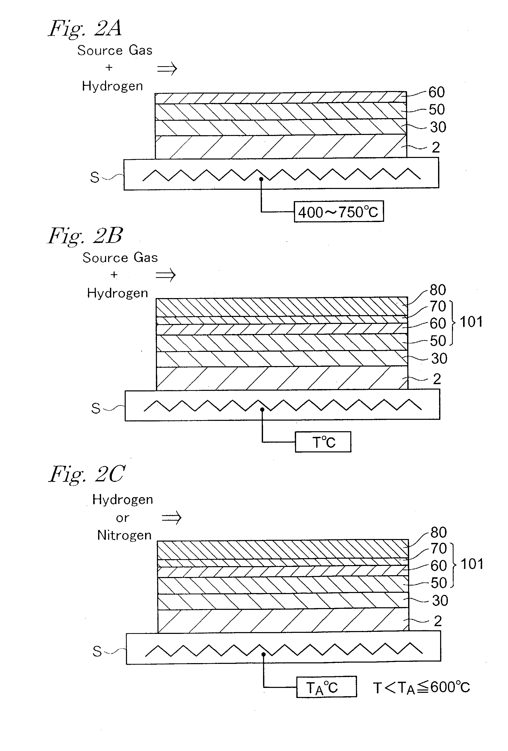
[0024] In embodiments, an HBT formed on an InP substrate is described. Elements identical to each other will be referred to with numerals identical to each other without overlapping explanations. In the drawings, dimensions such as layer thickness will not always reflect their explanation. Indices of surface and axis appearing in the drawings are exemplary and would contain their equivalent.

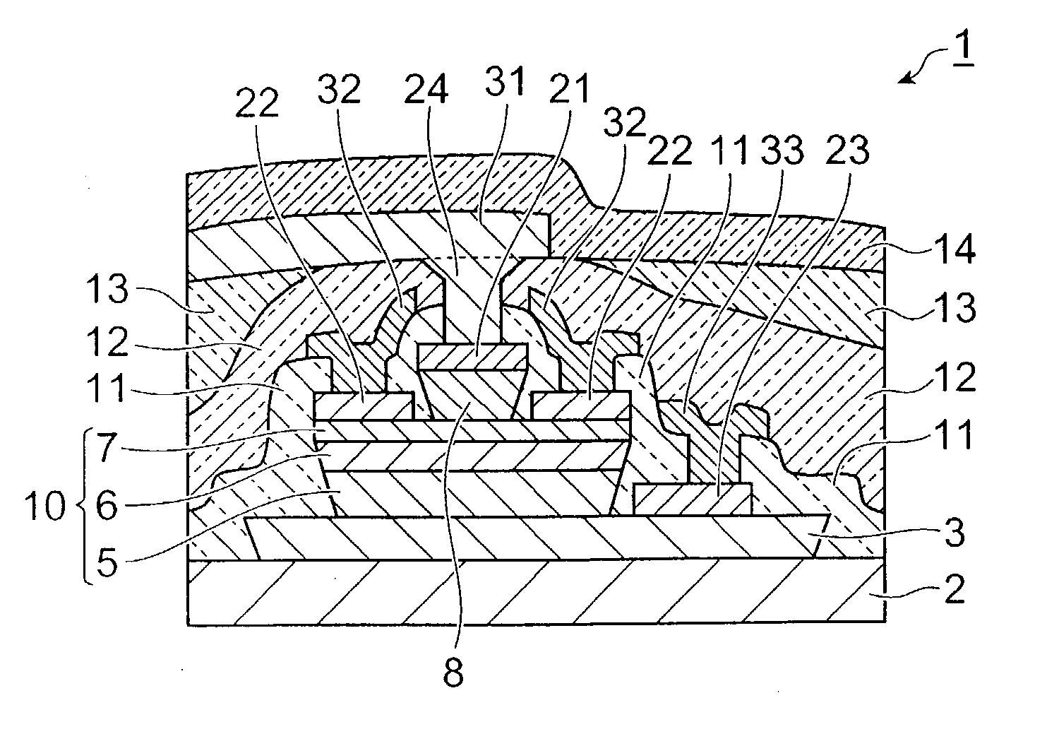
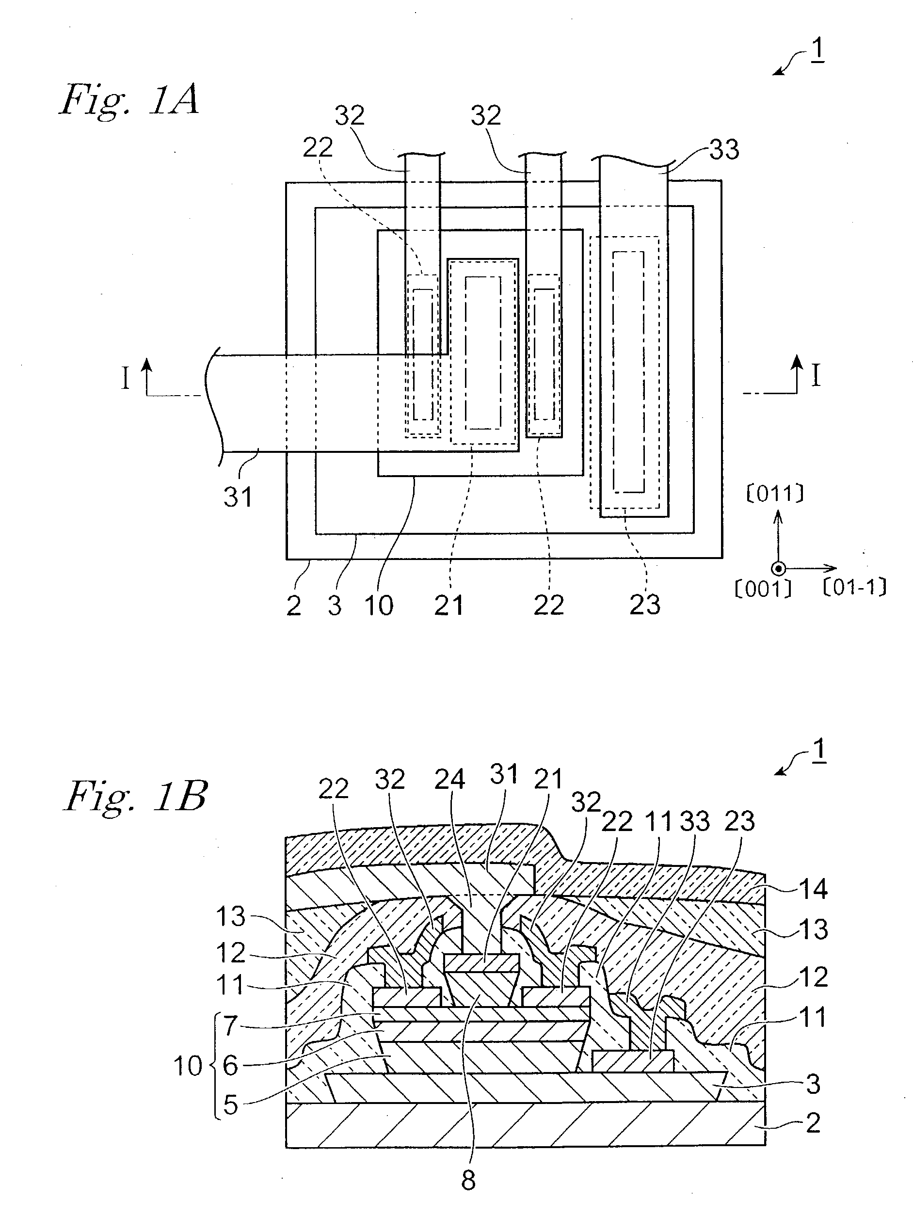
[0025] FIG. 1A is a plan view showing an HBT according to the present invention and FIG. 1B is a sectional taken along the line I-I in FIG. 1A, which extends along [01-1] crystal orientation. In FIG. 1B, the HBT 1 comprises a semi-insulating InP substrate 2, a sub-collector mesa formed on the substrate 2, a primary mesa 10 formed on the sub-collector mesa 3, and an emitter contact mesa 8 formed on the primary mesa 10. The primary mesa 10 contains a collector layer 5, a base laye...


PUM

PropertyMeasurementUnit
temperatureaaaaaaaaaa
lengthaaaaaaaaaa
widthaaaaaaaaaa

Abstract

This invention provides a method for manufacturing a hetero-junction bipolar transistor, in which a hole concentration of a base layer doped with carbon can be increased. The method comprises the following steps. 1) A sub-collector 30, a collector 50, a base 60 doped with carbon are sequentially grown after setting a semiconductor substrate on the stage in the growth chamber; 2) an emitter 70 and an emitter contact 80 are grown at a temperature T; and 3) grown layers are annealed at a temperature TA, where the relation of T<Ta<=600° is satisfied. This process enhances the activation of carbon atoms by dissociating hydrogen atoms captured in the base 60 to the ambience.

Description

[0001] 1. Field of the Invention[0002] This invention relates to a method for manufacturing a hetero-junction bipolar transistor.[0003] 2. Related Prior Art[0004] The hetero-junction bipolar transistor (HBT) has an attention for an amplifying device in a high-speed optical communication system due to its large current gain and an excellent high frequency performance. Since the HBT has an emitter with band gap energy greater than that of a base, a minority carrier injection from the base to the emitter is prevented. Therefore, even when a majority carrier concentration in the base is increased, the current gain of the transistor can be kept high. Moreover, to increase the majority carrier in the base can be tied up to a thinner base, thereby shortening a carrier drifting time and enhancing the high frequency performance.[0005] The HBT composed of group III-V semiconductor materials is likely to configure an n-p-n type transistor, because the mobility of electrons is far greater than ...

Claims


Application Information

Patent Timeline
Patent Type & Authority Applications(United States)
IPC IPC(8): H01L21/205H01L21/331H01L29/737
CPCH01L29/66318
Inventor HIRATSUKA, KENJI
Owner SUMITOMO ELECTRIC IND LTD
Why Eureka
Try Eureka