Photoconductor on active pixel image sensor

a photoconductor and image sensor technology, applied in the field of photoconductor on active pixel image sensor, can solve the problems of large energy consumption of small cameras using ccd sensors, occupied circuitry, and inability to use photo-sensing

Inactive Publication Date: 2004-02-26
E PHOCUS
View PDF0 Cites 74 Cited by
  • Summary
  • Abstract
  • Description
  • Claims
  • Application Information

AI Technical Summary

Benefits of technology

[0008] In particular preferred embodiments the sensor is a 0.3 mega-pixel (3.2 mm.times.2.4 mm, 640.times.480) array of 5-micron square pixels that is compatible with a lens of {fraction (1 / 4.5)} inch optical format. In these preferred embodiments the sensor along with focusing optics is incorporated into a cellular phone camera to permit transmission of visual images along with the voice communication. The result is an extremely low cost camera at high volume production that can be made extremely small (e.g., smaller than the human eye). High volume production costs for the above 0.3 mega-pixel camera are projected to be less than $10 per camera. Preferred embodiments also include infrared and ultraviolet cameras with high quantum efficiencies and fast response times and large pixel arrays such as a 2 million-pixel high definition television format sensor.

Problems solved by technology

One big drawback with CCD's is that the technique for producing CCD's is incompatible with other integrated circuit technology such as metal oxide semiconductor (MOS) and complementary metal oxide semi-conductor (CMOS) technology, so that processing circuits for the CCD arrays must be produced on chips separate from the CCD's.
The active circuitry consists of multiple transistors that are inter-connected by metal lines; as a result, the area occupied by the circuitry is opaque to visible light and cannot be used for photo-sensing.
Small cameras using CCD sensors typically consume large amounts of energy (as compared to cameras with CMOS sensors) and require high rail-to-rail voltage swings to operate CCD.
This can pose problems for today's mobile appliances, such as Cellular Phone and Personal Digital Assistant.
On the other hand, small cameras using CMOS sensors may provide a solution for energy consumption; but the traditional CMOS-based small cameras suffer low light sensing performance, which is intrinsic to the nature of CMOS APS sensors caused by shallow junction depth in the silicon substrate and its active transistor circuitry taking away the real estate preciously needed for photo-sensing.
Combining CMOS and MOS sensors with external processors can result in complexity and increase production costs.

Method used


Image

  • Photoconductor on active pixel image sensor
  • Photoconductor on active pixel image sensor
  • Photoconductor on active pixel image sensor

Examples


Embodiment Construction

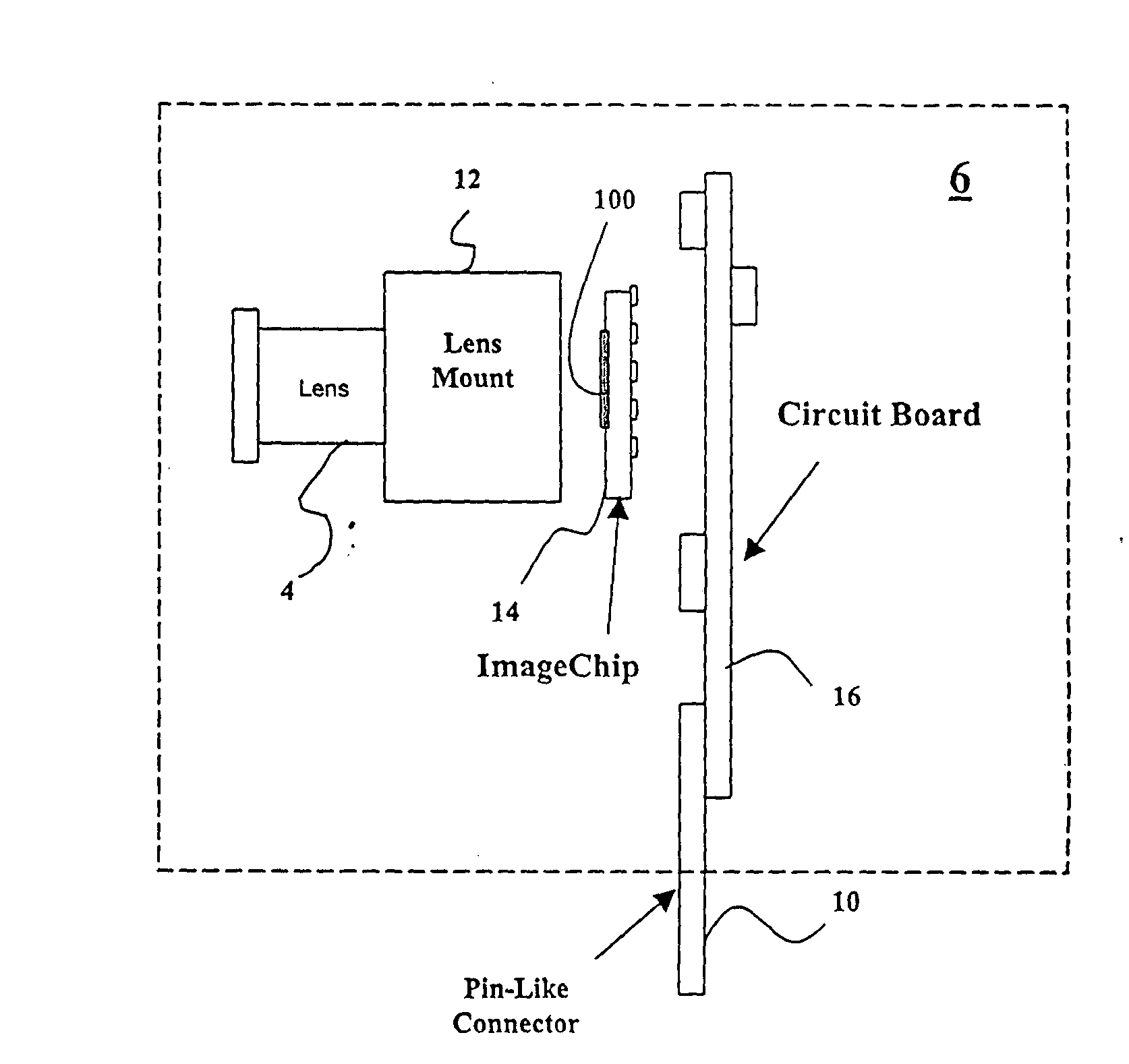
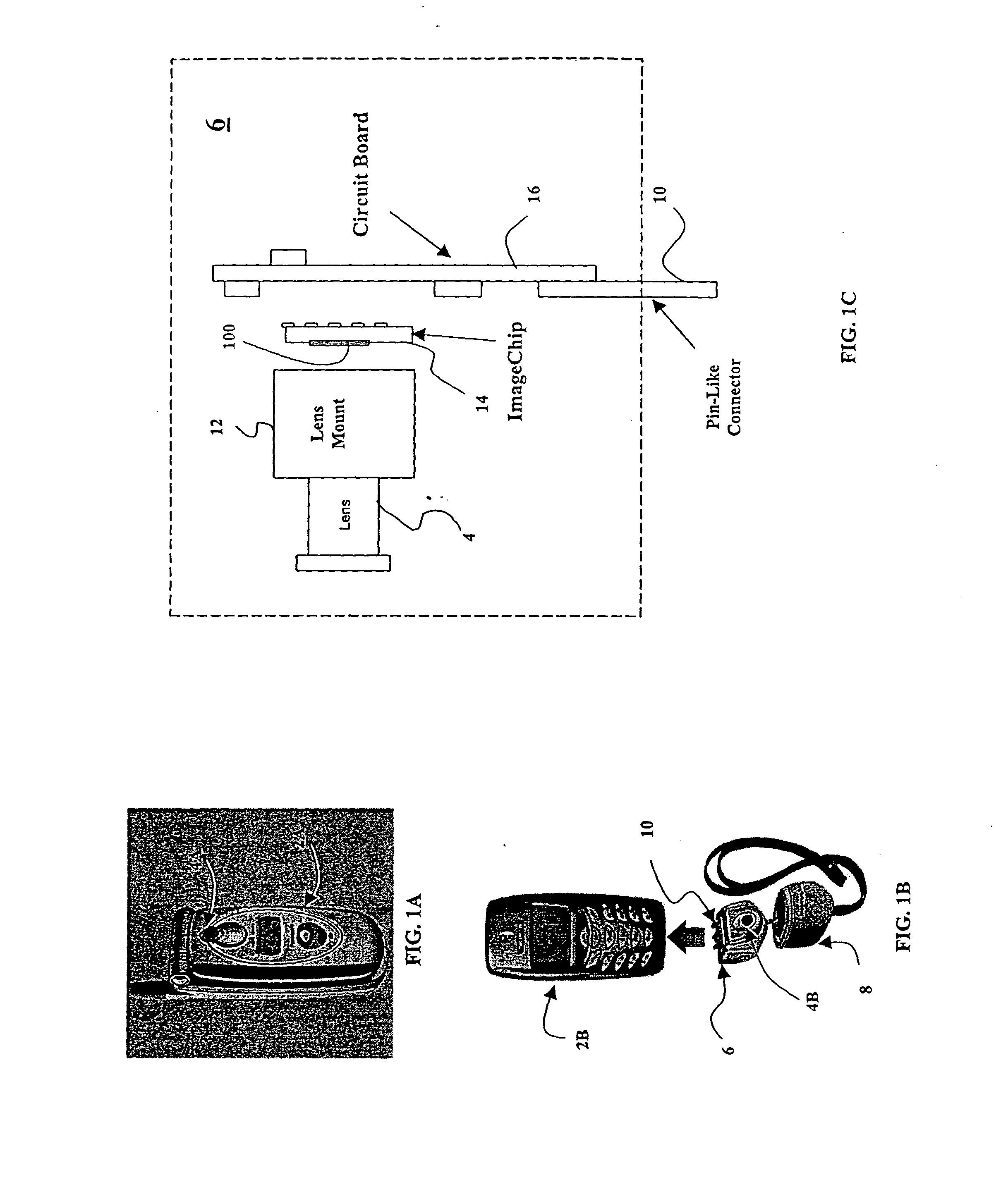
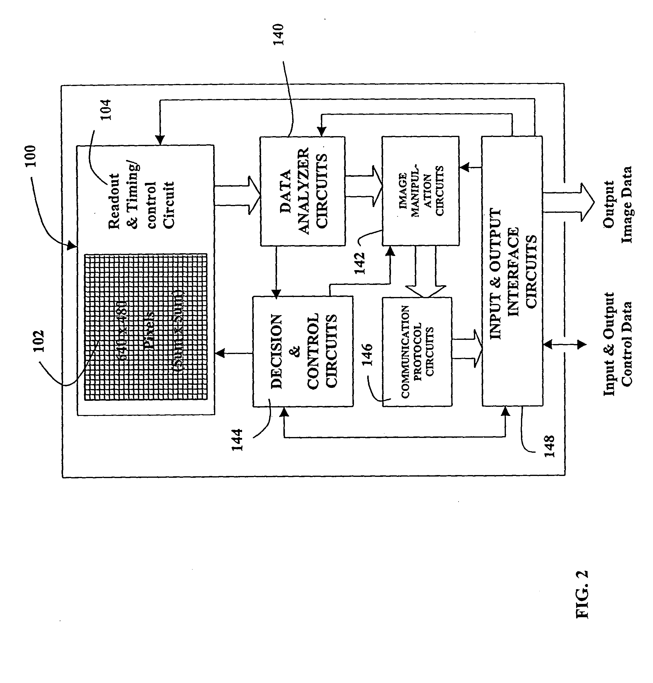
[0048] Single Chip Camera with Photo Conductor on Active Pixel Sensor A preferred embodiment of the present invention is a single chip camera with a sensor consisting of a photodiode array consisting of photoconductive layers on top of an active array of CMOS circuits. (Applicants refer to this sensor as a "POAP Sensor" the "POAP" referring to "Photoconductor On Active Pixel".) In this particular POAP sensor there are 307,200 pixels arranged in as a 640.times.480 pixel array and there is a transparent electrode on top of the photoconductive layers. The pixels are 5 microns.times.5 microns and the packing fraction is approximately 100 percent. The active dimensions of the sensor are 3.2 mm.times.2.4 mm and a preferred lens unit is a standard lens with a {fraction (1 / 4.5)} inch optical format. A preferred application of the camera is as a component of a cellular phone as shown in FIGS. 1A and 1B. In the 1A drawing the camera is an integral part of the phone 2A and the lens is shown at...


PUM


Abstract

A MOS or CMOS based photoconductor on active pixel image sensor. Thin layers of semi-conductor material, doped to PIN or NIP photoconducting layers, located above MOS and / or CMOS pixel circuits produce an array of layered photodiodes. Positive and negative charges produced in the layered photodiodes are collected and stored as electrical charges in the MOS and / or CMOS pixel circuits. The present invention also provides additional MOS or CMOS circuits for reading out the charges and for converting the charges into images. With the layered photodiode of each pixel fabricated as continuous layers of charge generating material on top of the MOS and / or CMOS pixel circuits, extremely small pixels are possible with almost 100 percent packing factors. MOS and CMOS fabrication techniques permit sensor fabrication at very low costs. In preferred embodiments all of the sensor circuits are incorporated on or in a single crystalline substrate along with the sensor pixel circuits. Techniques are disclosed for tailoring the spectral response of the sensor for particular applications.

Description

[0001] This application is a continuation in part of U.S. Pat. application Ser. No. 10 / 072,637 filed Feb. 5, 2002, Ser. No. 10 / 229,953 filed Aug. 27, 2002, Ser. No. 10 / 229,954 filed Aug. 27, 2002, Ser. No. 10 / 229,955 filed Aug. 27, 2002, Ser. No. 10 / 229,956 filed Aug. 27, 2002 and Ser. No. 10 / 371,618, filed Feb. 22, 2003. The present invention relates to image sensors and in particular to MOS and CMOS based image sensors.BACKGROUND OF THE INVENTION[0002] A typical electronic image sensor is comprised of an array of a large number of very small light detectors, together called a "pixel array". These sensors typically generate electronic signals representative of each pixel that have amplitudes that are proportional to the intensity of the light received by each of the detectors in the array. In electronic cameras imaging components produce an optical image of a scene onto the pixel array. The electronic image sensor converts the optical image into a set of electronic signals. These e...

Claims


Application Information

Patent Timeline
Patent Type & Authority Applications(United States)
IPC IPC(8): H01L27/00H01L27/146H01L29/76H01L31/00H01L31/062H01L31/105H01L31/113
CPCH04N5/378H04N5/37455H01L27/14621H01L27/1463H01L27/14632H01L27/14636H01L27/14643H01L27/14645H01L27/14687H01L31/1055H01L31/113H04N3/155H04N5/2351H04N5/2353H04N5/365H01L27/14609H04N23/71H04N23/73H04N25/67H04N25/772H04N25/75
Inventor HSIEH, TZU-CHIANGCHAO, CALVIN
Owner E PHOCUS
Why Eureka
Try Eureka