

Semiconductor device and method of crystal growth
Inactive Publication Date: 2004-05-06
SHARP KK
View PDF1 Cites 15 Cited by
- Summary
- Abstract
- Description
- Claims
- Application Information
AI Technical Summary
Benefits of technology
[0007] The present invention was made in order to solve the above problem. That is, an objective is to provide a mixed crystal composition that can remarkably improve light emission characteristics of a III-V compound semiconductor material wherein N and other V-group elements (As, P, etc.) are intermixed, as well as to provide a semiconductor device having superior characteristics. Furthermore, a method of fabricating such a crystal is also provided.
Problems solved by technology
Thus, it becomes difficult to mix nitrogen in a crystal.
For that reason, as the N mole fraction in the mixed crystal increases, a problem of rapid deterioration of light-emitting characteristics occurs.
Method used
View moreImage
Smart ImageViewing Examples

Examples
embodiment 1
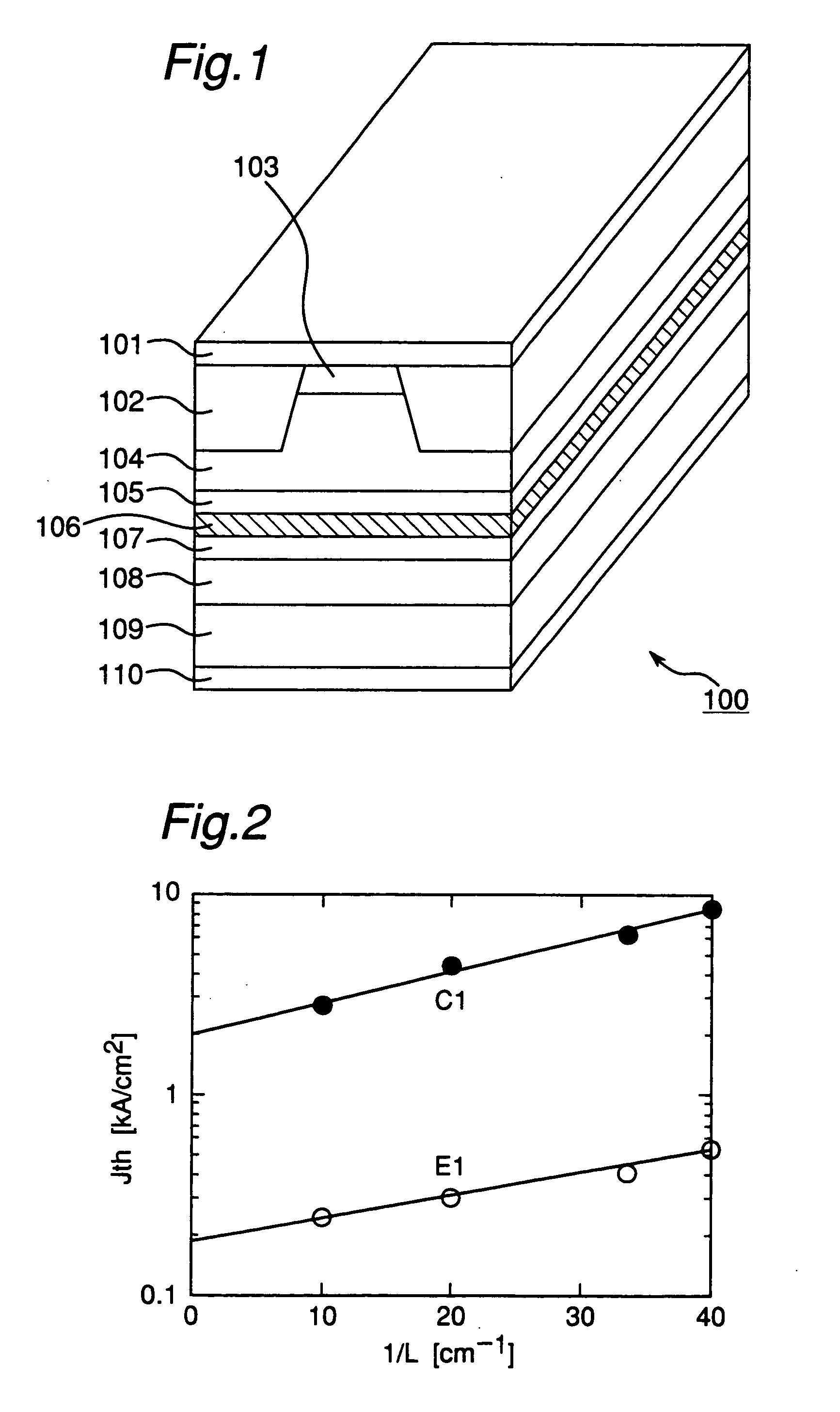
. As is apparent from FIG. 2, the threshold current density J.sub.th Of the semiconductor laser element of Embodiment 1 extrapolated when L converges to infinity (L.fwdarw..infin.) (that is, 1 / L.fwdarw.0) was 0.19 kA / cm.sup.2.
embodiments 2 and 3
[0068] (Embodiments 2 and 3)
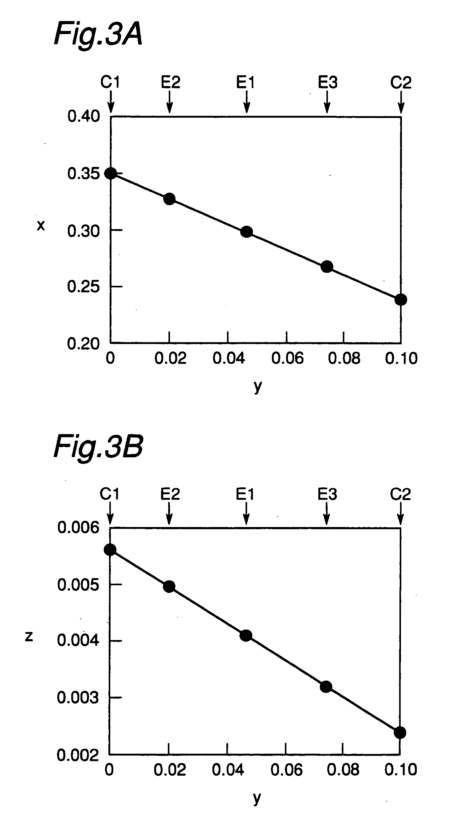
[0069] Semiconductor lasers wherein the well layer 106 of the semiconductor laser structure described in detail in Embodiment 1 was replaced with:
embodiment 2
[0070] i-Ga.sub.0.67In.sub.0.33N.sub.0.0052As.sub.0.9748Sb.sub.0.02, 7 nm, strain amount of 2.4% in Embodiment 2, and
Login to View More PUM
 Abstract
A semiconductor device (100) has, as its well layer, a III-V compound semiconductor layer (106) containing, as V-group components, nitrogen, antimony, and one or more V-group elements other than nitrogen and antimony to improve emission characteristics. Such a III-V compound semiconductor layer is formed by repeating a cycle including a process of simultaneously supplying a plurality of sources containing at lest indium, and a process of simultaneously supplying a plurality of sources not containing indium but containing antimony.
Description
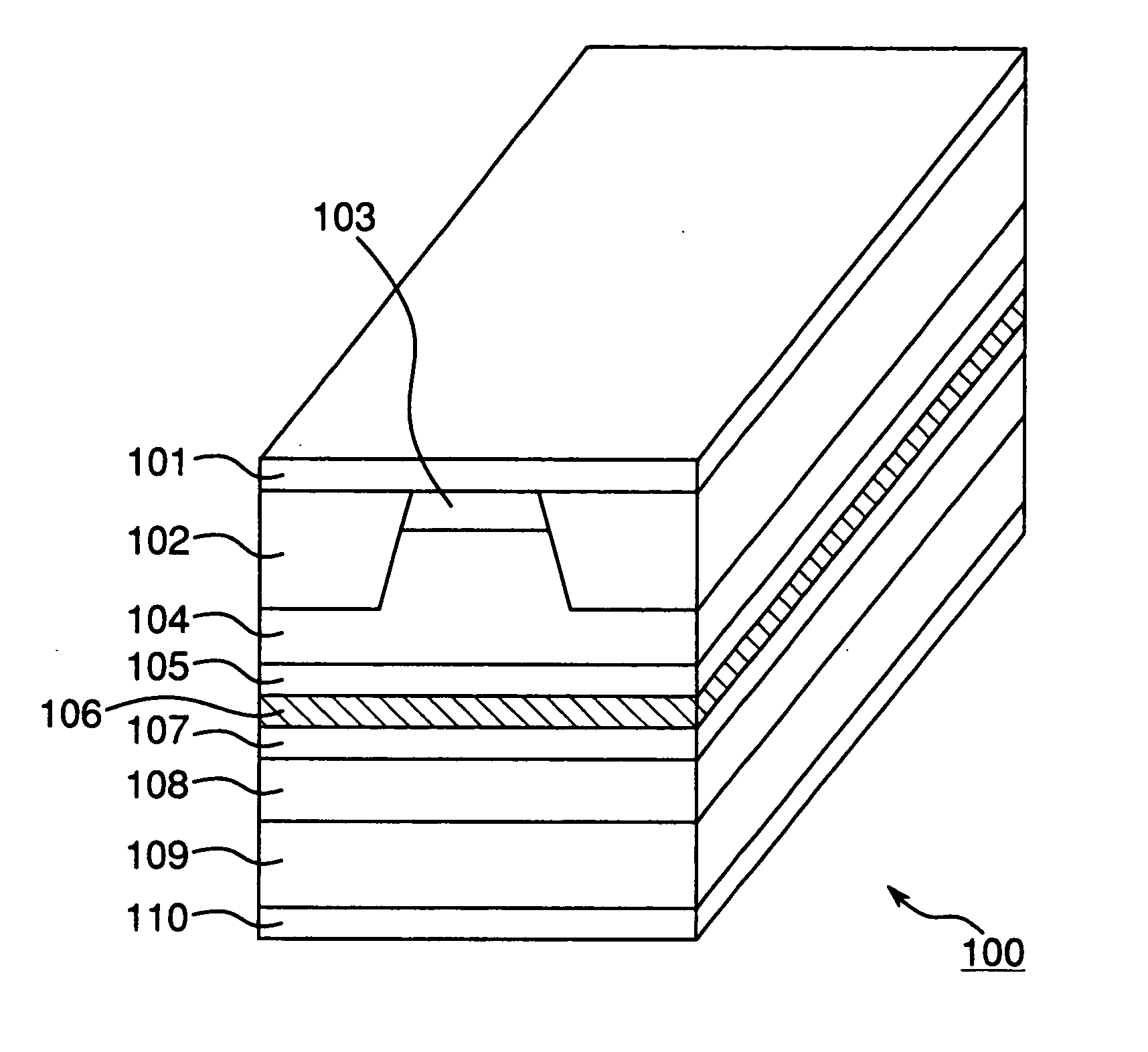
[0001] The present invention relates to a semiconductor device using a III-V compound semiconductor crystal containing, as V-group composition, nitrogen and at least one other V-group element, and a method of growing the crystal.[0002] Recently, as a new material system that would greatly expand the utilization field of III-V compound semiconductors, there has been proposed a III-V compound semiconductor material containing, as the V-group composition, nitrogen (N) at a mole fraction of not more than several % of the V-group content, and arsenic (As) and phosphorus (P). V-group elements such as As and P greatly differ from N in the atomic radius (N: 0.070 nm, As: 0.118 nm, P: 0.110 nm), and in the electronegativity (N: 3.5, As: 2.4, P: 2.5). Thus, by intermixing N and As, or N and P, or N and As and P, a singular physical property is generated. For example, in the case of GaInNAs, which is presumed to be an intermixture of GaInAs and several percent of GaInN having a larger bandgap ...
Claims
Login to View More Application Information
Patent Timeline
 IPC IPC(8): H01L21/18H01L21/203H01L21/205H01S5/10H01S5/223H01S5/323H01S5/343
CPCB82Y20/00H01S2304/00H01L21/02395H01L21/02458H01L21/02463H01L21/02466H01L21/0254H01L21/02543H01L21/02546H01L21/02549H01L21/0262H01L21/02631H01L21/182H01S5/1003H01S5/2231H01S5/32366H01S5/343H01S5/34306H01S5/34346H01L21/0237
InventorTAKAHASHI, KOJI
OwnerSHARP KK