
Silocon-controlled rectifier with dynamic holding voltage for on-chip electrostatic discharge protection

Inactive Publication Date: 2004-05-27
IND TECH RES INST
View PDF10 Cites 36 Cited by
  • Summary
  • Abstract
  • Description
  • Claims
  • Application Information

AI Technical Summary

Benefits of technology

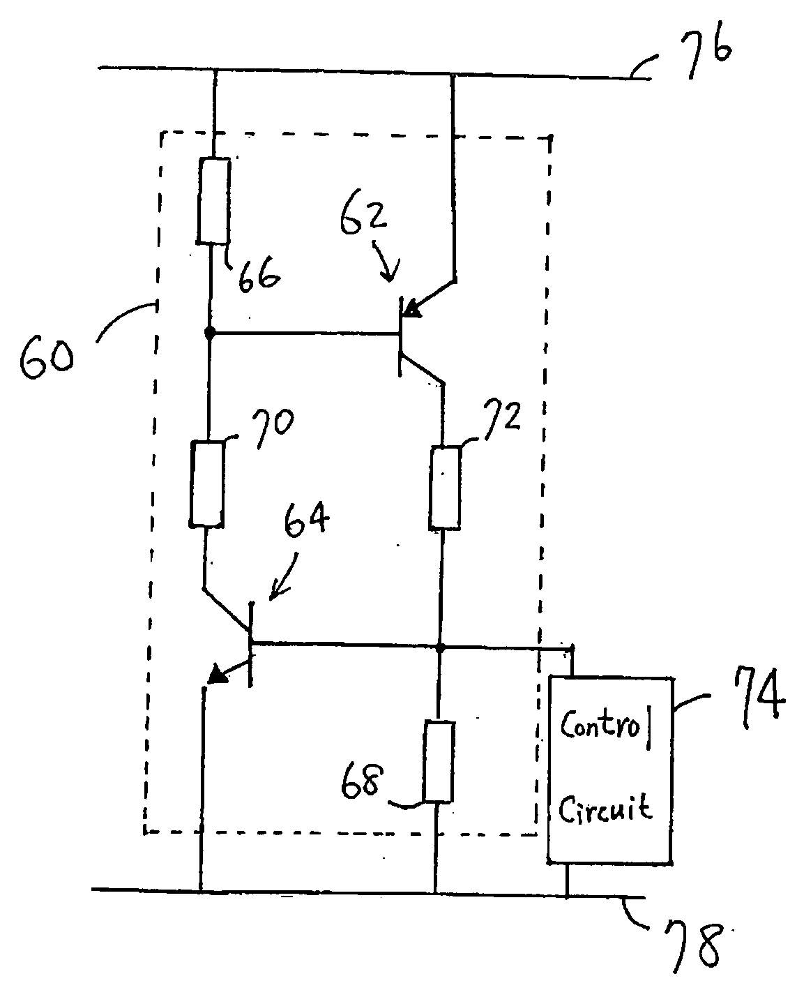
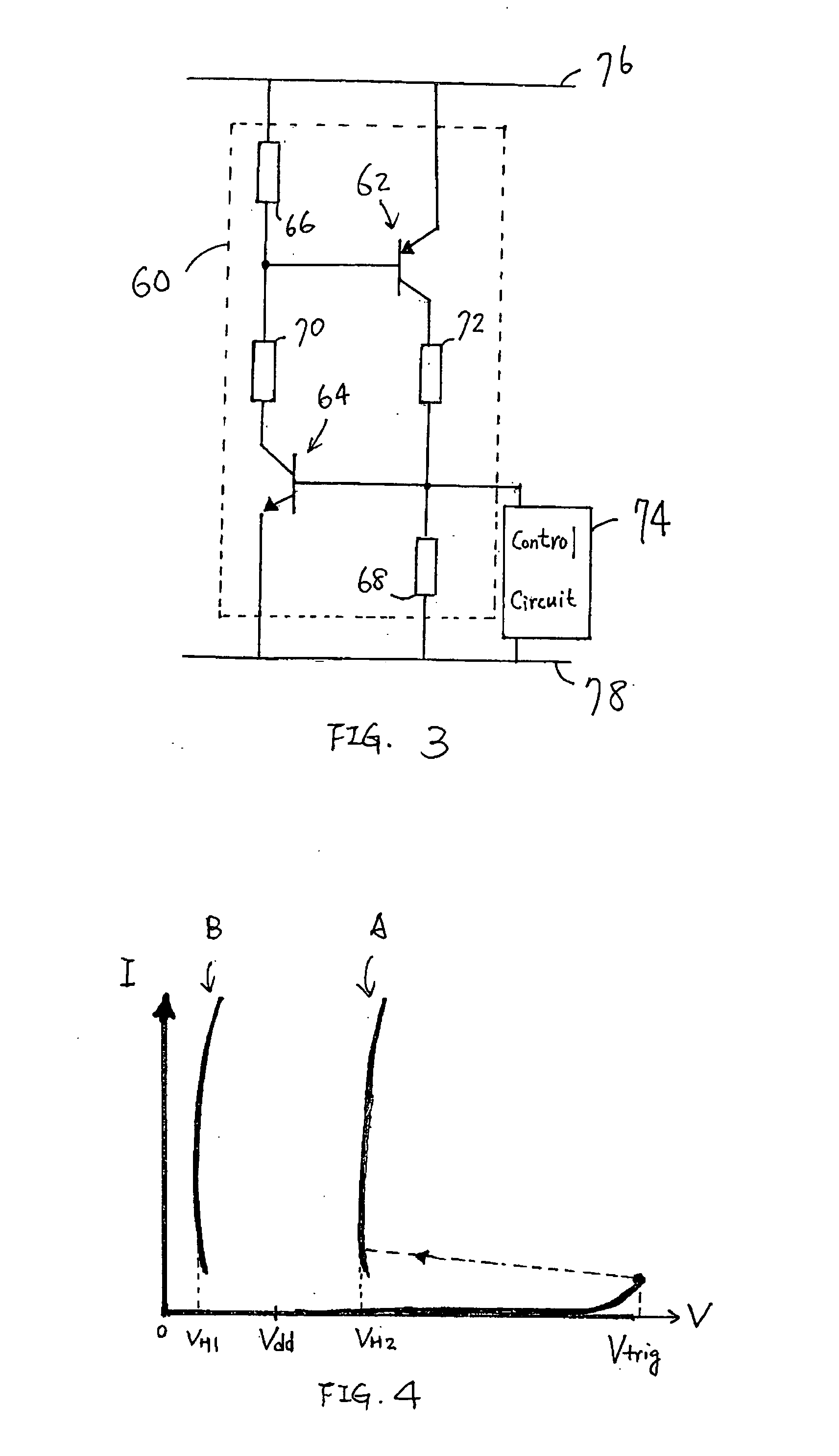
[0020] Still in accordance with the present invention, there is provided an integrated circuit for electrostatic discharge (ESD) protection that comprises a first voltage line of a first voltage level, a second voltage line of a second voltage level, a plurality of contact pads, a plurality of silicon-controlled rectifiers (SCR), each of the SCRs including a p-type transistor and an n-type transistor integrally formed with the SCR, and a control circuit providing a first holding voltage through the p-type and n-type transistors to the SCRs to keep the SCRs from latching-up, and providing a second holding voltage through the p-type and n-type transistors to the SCRs to keep the SCRs in the latch-up state during an ESD event that an ESD pulse appears on the first voltage line or one of the contact pads.
[0021] Yet still in accordance with the present invention, there is provided a method of electrostatic discharge protection that comprises providing a silicon-controlled rectifier (SCR) having a holding voltage, integrally forming a first transistor of a first type with the SCR including a first gate, integrally forming a second transistor of a second type with the SCR including a second gate, and providing a first signal to the first and second gates to raise the holding voltage of the SCR to keep the SCR from latching up, and providing a second signal to the first and second gates to lower the holding voltage of the SCR to keep the SCR in the latch-up state.
[0022] Further still in accordance with the present invention, there is provided a method of providing electrostatic discharge (ESD) protection for internal circuits that comprises providing a first voltage line of a first voltage level, providing a second voltage line of a second voltage level, providing a plurality of contact pads, providing a plurality of silicon-controlled rectifiers (SCR), each of the SCRs including a p-type transistor and an n-type transistor formed integrally with the SCR, and providing a first holding voltage through the p-type and n-type transistors to the SCRs to keep the SCRs from latching-up, and providing a second holding voltage through the p-type and n-type transistors to the SCRs to keep the SCRs in the latch-up state during an ESD event that an ESD pulse appears on the first voltage line or one of the contact pads.

Problems solved by technology

A semiconductor integrated circuit ("IC") is susceptible to an electrostatic discharge ("ESD") event, which may cause damage to the IC, such as one with advanced metal-oxide-semiconductor ("MOS") transistors.
These MOS transistors, manufactured using quarter-submicron complemental metal-oxide-semiconductor ("CMOS") processes with lightly-doped drain ("LDD") structures and clad silicide diffusions, are more vulnerable to ESD.
An IC is susceptible to the HBM and MM built-up during fabrication, transportation, or handling.
Moreover, SCRs are liable to latch-up or transient latch-up during normal operations due to noise such as a power surge or spike.
Upon an SCR latch-up during normal operations, an IC to be protected by the SCR ceases to function properly or may even be permanently damaged.
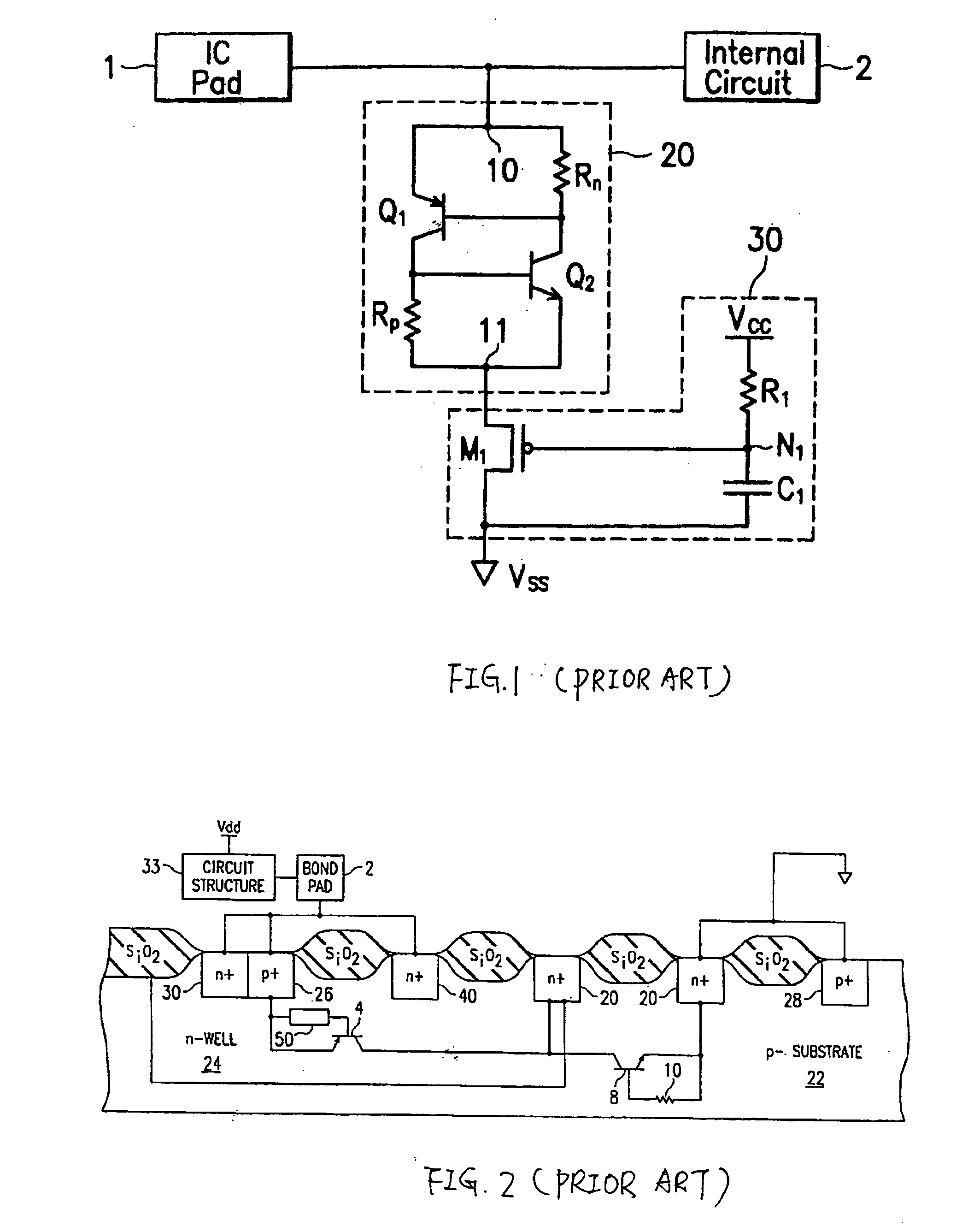
Transistor M1 that occupies a large chip area is not economically acceptable and impracticable in today's limited layout area required for an ESD protection device.
Resistor 50 allows more current to flow through and thus makes the pnp bipolar transistor difficult to turn on.
Although the '404 patent is able to raise the holding voltage of the SCR to above a power supply voltage, Vdd, such a holding voltage is not adjustable once it is determined.
An SCR with such a fixed, high holding voltage is unable to sustain a large ESD current.
Further, an SCR with a high holding voltage usually clamps ESD stress at a voltage higher than the power supply voltage Vdd, causing potentially destructive effects on internal circuits.

Method used


Image

  • Silocon-controlled rectifier with dynamic holding voltage for on-chip electrostatic discharge protection
  • Silocon-controlled rectifier with dynamic holding voltage for on-chip electrostatic discharge protection
  • Silocon-controlled rectifier with dynamic holding voltage for on-chip electrostatic discharge protection

Examples


Embodiment Construction

[0002] 1. Field of the Invention

[0003] This invention pertains in general to a semiconductor device and, more particularly, to an electrostatic discharge protection device that is immune to latch-up during normal operations.

[0004] 2. Background of the Invention

[0005] A semiconductor integrated circuit ("IC") is susceptible to an electrostatic discharge ("ESD") event, which may cause damage to the IC, such as one with advanced metal-oxide-semiconductor ("MOS") transistors. Advanced MOS transistors have traditionally required certain properties such as short channel lengths, low threshold voltages, and thin gate oxide layers. These MOS transistors, manufactured using quarter-submicron complemental metal-oxide-semiconductor ("CMOS") processes with lightly-doped drain ("LDD") structures and clad silicide diffusions, are more vulnerable to ESD.

[0006] An ESD event is an electrical discharge of a current (positive or negative) for a short duration during which a large amount of current is ...


PUM


Abstract

An integrated circuit for electrostatic discharge (ESD) protection that comprises a silicon-controlled rectifier (SCR), a first transistor of a first type integrally formed with the SCR including a first gate, a second transistor of a second type integrally formed with the SCR including a second gate, and a control circuit in response to a first voltage applied to the first and second gates providing a first holding voltage to the SCR to keep the SCR from latching-up, and in response to a second voltage applied to the first and second gates providing a second holding voltage to the SCR to keep the SCR in the latch-up state.

Description

[0001] This application is a Continuation In Part of U.S. application Ser. No. 10 / 400,874 filed Mar. 28, 2003, whose content is incorporated herein by reference in its entirety.DESCRIPTION OF THE INVENTION[0002] 1. Field of the Invention[0003] This invention pertains in general to a semiconductor device and, more particularly, to an electrostatic discharge protection device that is immune to latch-up during normal operations.[0004] 2. Background of the Invention[0005] A semiconductor integrated circuit ("IC") is susceptible to an electrostatic discharge ("ESD") event, which may cause damage to the IC, such as one with advanced metal-oxide-semiconductor ("MOS") transistors. Advanced MOS transistors have traditionally required certain properties such as short channel lengths, low threshold voltages, and thin gate oxide layers. These MOS transistors, manufactured using quarter-submicron complemental metal-oxide-semiconductor ("CMOS") processes with lightly-doped drain ("LDD") structure...

Claims


Application Information

Patent Timeline
IPC IPC(8): H01L27/02
CPCH01L27/0262
Inventor CHEN, ZI-PINGCHANG, CHYH-YIHKER, MING-DOU
Owner IND TECH RES INST
Learn More