Adhesion between dielectric materials

a dielectric material and adhesive technology, applied in the direction of ceramic layered products, transportation and packaging, chemistry apparatus and processes, etc., can solve the problems of affecting the switching speed of transistors, affecting the performance and reliability of chips, and poor yield at assembly and packaging

Inactive Publication Date: 2004-05-27
OLOUGHLIN JENNIFER +2
View PDF9 Cites 251 Cited by
  • Summary
  • Abstract
  • Description
  • Claims
  • Application Information

AI Technical Summary

Problems solved by technology

The scaling down of transistors and wiring to comply with Moore's Law may degrade the performance and reliability of the chip if it is not accomplished properly.
For example, the switching speed of the transistors may be adversely impacted if the resistance-capacitance (RC) product delay in the wiring is too large.
However, adhesion at an interface between two dielectric materials may be inadequate, resulting in poor yield at assembly and packaging from cracking and delamination.

Method used


Image

  • Adhesion between dielectric materials
  • Adhesion between dielectric materials
  • Adhesion between dielectric materials

Examples


first embodiment

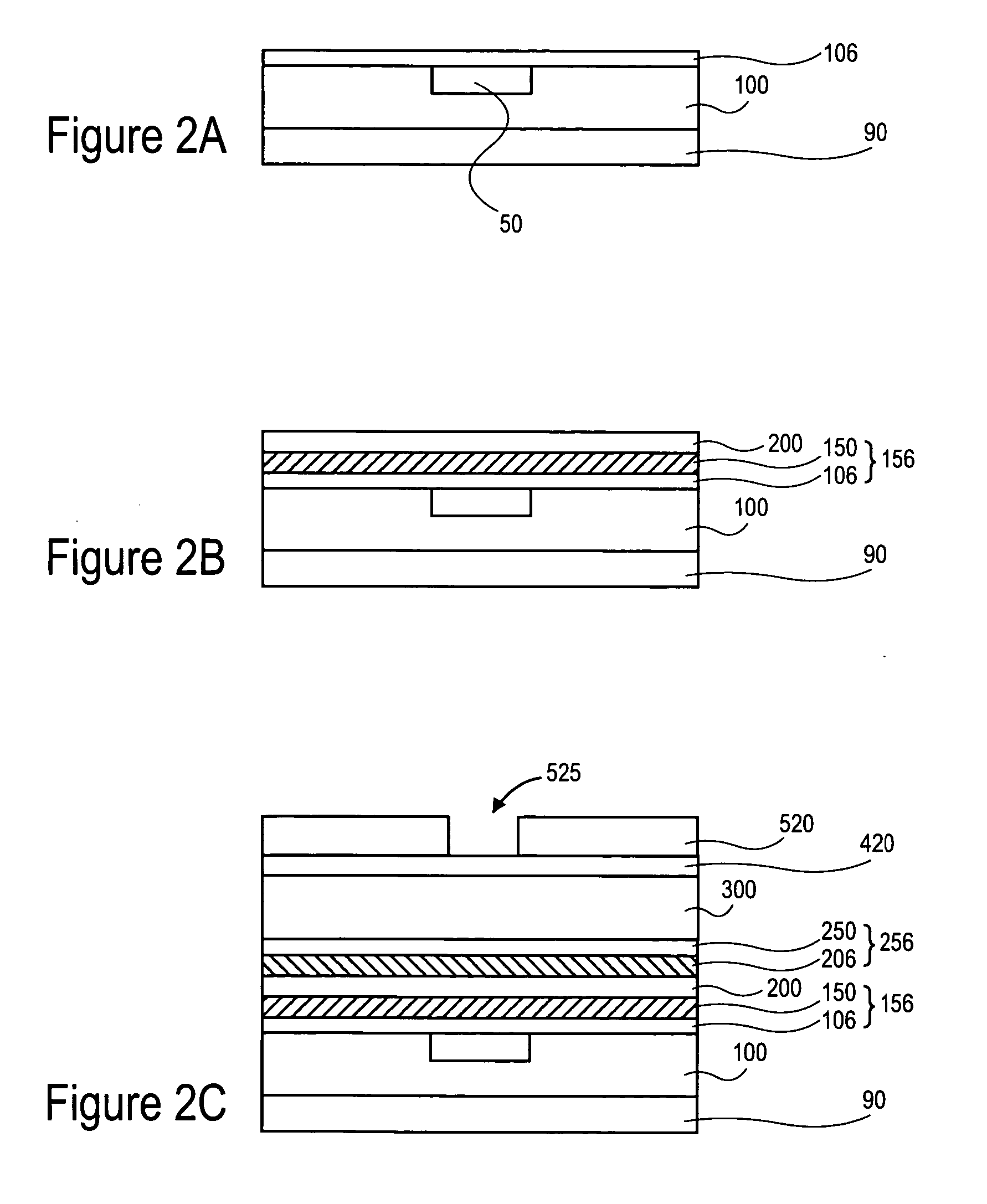
[0127] In the present invention, the CMP process involves three polishes. Each polish includes optimization of the polish rates and the polish selectivity by using a different combination of slurry, pad, and polish tool parameters. The first polish removes most of the overburden of the conductor layer 700. The second polish planarizes the remaining conductor layer 700 and the portion of the seed layer 650 that is located over the barrier layer 630. The polish rate of the conductor layer 700 in the first polish and the second polish may be selected from a range of about 900-13,000 Angstroms per minute. The third polish removes the portion of the barrier layer 630 that is located over the upper surface 547 of the ILD 300.

[0128] The polish rate of the barrier layer 630 may be selected from a range of about 100-1,000 Angstroms per minute. In an embodiment of the present invention, the polish of the barrier layer 630 may be highly selective relative to the ILD 300. A selective process pr...

second embodiment

[0130] In the present invention, the CMP process involves two polishes. The first polish removes all of the overburden of the conductor layer 700 and planarizes the conductor layer 700 and the portion of the seed layer 650 that is located over the barrier layer 630. The second polish removes the portion of the barrier layer 630 over the upper surface 547 of the ILD 300.

third embodiment

[0131] In the present invention, the CMP process involves one polish to remove all of the overburden of the conductor layer 700, as well as the portions of the seed layer 630 and the barrier layer 650 that are located over the ILD 300.

[0132] The material and mechanical properties of the ILD 300 must be sufficient to prevent any deformation, fracture, or delamination of the ILD 300 during the CMP process that is used to planarize the conductor layer 700. Otherwise, electrical shorts and other polish-induced defects may occur, thus degrading yield.

[0133] The mechanical strength of the ILD 300 depends on the mechanical strength of the bulk material forming the ILD 300. If the ILD 300 is porous, the mechanical strength of the ILD 300 also depends on the porosity and the pore size, shape, and distribution. Young's modulus of elasticity is a measurement of mechanical strength of a material. In a first embodiment, the ILD 300 is porous with a Young's modulus of elasticity of about 3 GigaPa...


PUM

PropertyMeasurementUnit
thicknessaaaaaaaaaa
thicknessaaaaaaaaaa
temperatureaaaaaaaaaa

Abstract

The present invention discloses a method including: determining whether a surface of a dielectric layer is reactive; activating the surface if the surface is not reactive; performing a cycle on the surface, the cycle including: reacting the surface with a metal; and activating the metal. The present invention also discloses a structure including: a substrate; a first interlayer dielectric located over the substrate; a first adhesion promoter layer located over the first interlayer dielectric; an etch stop layer located over the first adhesion promoter layer; a second adhesion promoter layer located over the etch stop layer; and a second interlayer dielectric located over the second adhesion promoter layer.

Description

[0001] 1. Field of the Invention[0002] The present invention relates to the field of semiconductor integrated circuit (IC) manufacturing, and, more specifically, to a method of improving adhesion at an interface between dielectric materials, as well as, a structure including an adhesion promoter layer at the interface between dielectric materials.[0003] 2. Discussion of Related Art[0004] Gordon Moore first suggested in 1965 that the pace of technology innovation would double the number of transistors per unit area on a chip every 18 months. Over the ensuing decades, the semiconductor industry has adhered closely to Moore's Law in improving device density.[0005] Maintaining such an aggressive schedule for each device generation has required continual enhancements at the corresponding technology node. Additive processes using ion implantation, annealing, oxidation, and deposition had to be enhanced to deliver the requisite doping profiles and film stacks. Subtractive processes using p...

Claims


Application Information

Patent Timeline
Patent Type & Authority Applications(United States)
IPC IPC(8): H01L21/314H01L21/768
CPCH01L21/3141H01L21/76801H01L21/76808Y10T428/24926H01L21/76832H01L21/76834Y10T428/24917H01L21/76813H01L21/02211H01L21/02126H01L21/02216H01L21/02304H01L21/0228H01L21/02203H01L21/02282H01L21/02274
Inventor O'LOUGHLIN, JENNIFEROTT, ANDREW W.TUFTS, BRUCE J.
Owner OLOUGHLIN JENNIFER
Why Eureka
Try Eureka