Clock converter and electronic apparatus with the same

a converter and electronic equipment technology, applied in the direction of oscillator generators, pulse automatic control, pulse generation by logic circuits, etc., can solve the problems of generating jitter in the output signal, unstable feedback signal of pll feedback loop, and inability to reduce jitter

Inactive Publication Date: 2004-06-24
SEIKO EPSON CORP
View PDF4 Cites 10 Cited by
  • Summary
  • Abstract
  • Description
  • Claims
  • Application Information

AI Technical Summary

Problems solved by technology

Therefore, a PLL feedback signal by a PLL feedback loop becomes unstable.
However, in order to provide such means, it is necessary to determine component constants by cut and try caused by actual load and to add a large number of parts.
Accordingly, spurious or noise exists in an output signal to thus generate jitter in the output signal.
Therefore, it is impossible to reduce jitter.
However, it causes various problems as follows.
Firstly, because a power source and a ground in each functional block in FIG. 10 are shared and have low impedance, when the electric potential of the power source or the ground changes, noise overlaps, thus mutually influencing each functional block.
Therefore, it is impossible to isolate the parts from each other because the parts are close to each other.
Accordingly, the parts are easily electronically coupled or capacitively coupled with

Method used


Image

  • Clock converter and electronic apparatus with the same
  • Clock converter and electronic apparatus with the same
  • Clock converter and electronic apparatus with the same

Examples


second example

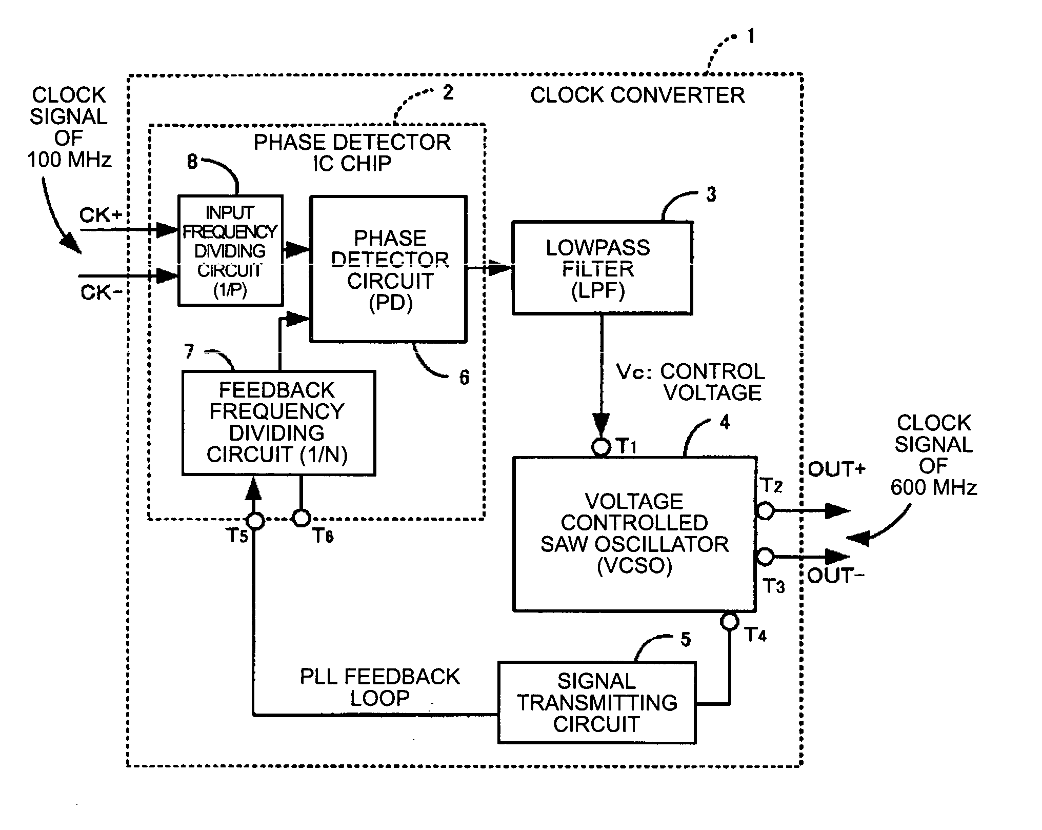
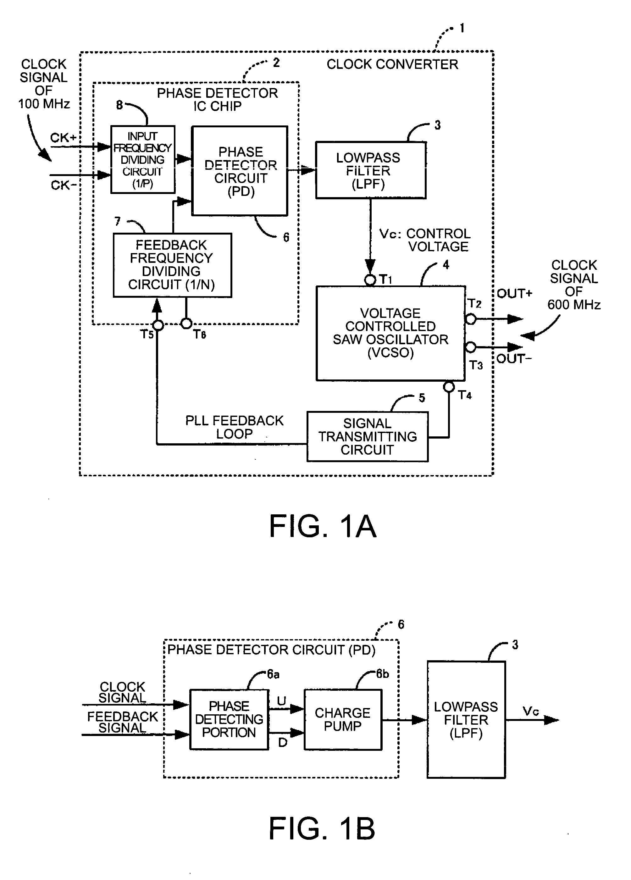
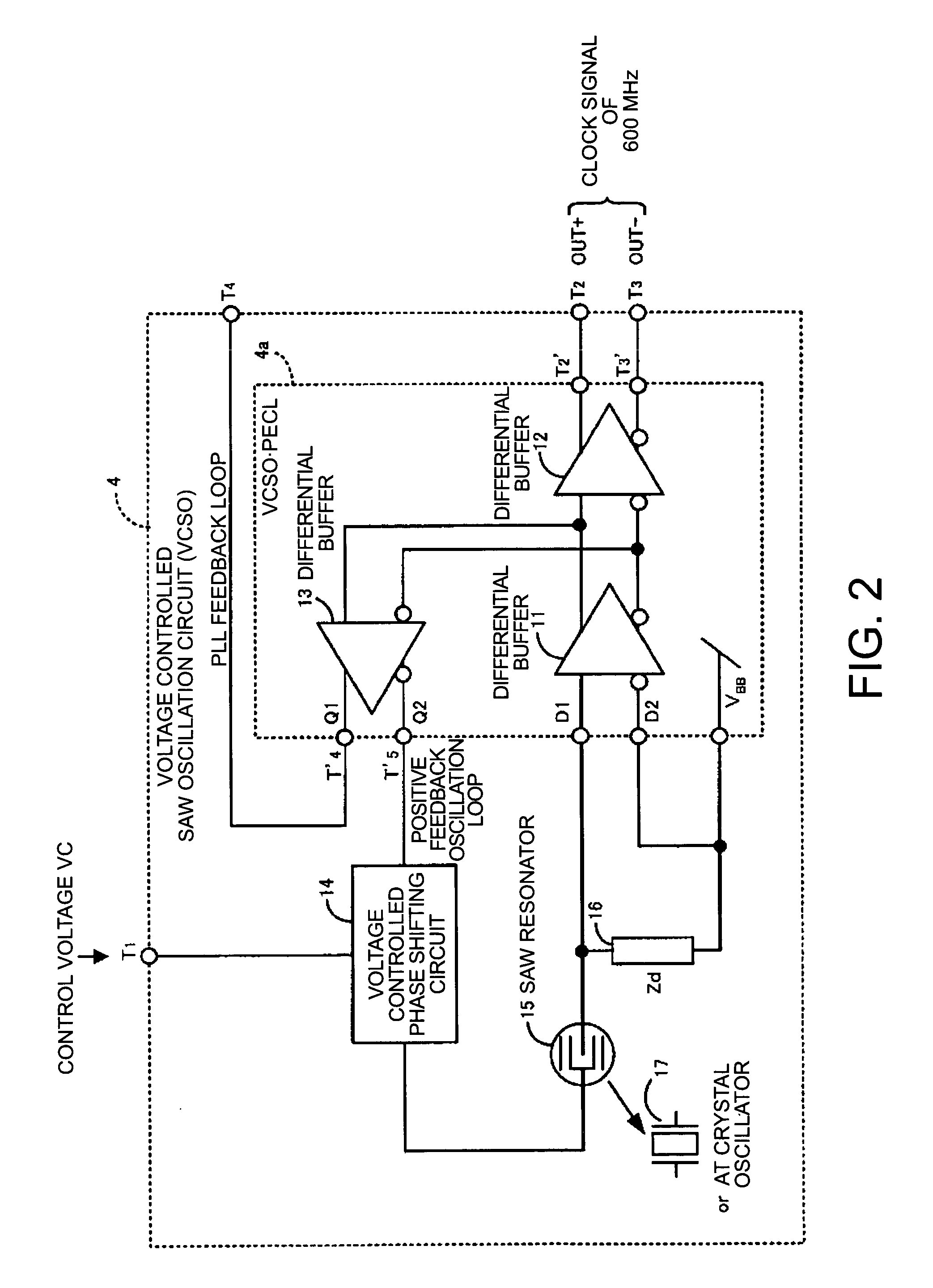
[0083] A signal transmitting circuit in cases where the differential amplifying circuit of the VCSO is the PECL and the differential amplifying circuit of the feedback frequency dividing circuit 7 is the CMOS circuit will now be described. FIG. 7 is a block diagram of the signal transmitting circuit inserted between the PECL of the output step of the VCSO and the differential CMOS of the input step of the feedback frequency dividing circuit of the phase detector IC chip in the clock converter shown in FIG. 1. The signal transmitting circuit of FIG. 7 illustrates the interface between the VCSO.multidot.PECL 4a of the output step of the VCSO 4 and the feedback frequency dividing circuit.multidot.differential CMOS 7b of the input step of the feedback frequency dividing circuit 7. One PLL feedback loop between the output terminal T4 of the VCSO.multidot.PECL 4a and the input terminal T5 of the feedback frequency dividing circuit.multidot.differential CMOS 7b is coupled through an AC cou...

first modification

[0098] First Modification

[0099] Furthermore, the case where the oscillation circuit is used for the network-dedicated optical transceiver module is described, but the oscillation circuit can be applied to various electronic apparatuses, such as mobile telephones and radio communication apparatuses, which require the oscillation circuit, in particular, a high frequency oscillation circuit.

second modification

[0100] Second Modification

[0101] Moreover, in principle, the positive feedback loop is formed in the order of the SAW resonator.fwdarw.an amplifier (including a feedback buffer amplifier).fwdarw.the voltage controlled phase shifting circuit. However, the positive feedback loop may be formed such that the position of the SAW resonator is exchanged for the position of the voltage controlled phase shifting circuit in the positive feedback loop.


PUM


Abstract

A voltage controlled oscillating means in a clock converter outputs a positive feedback signal for a positive feedback loop from one output terminal of buffer means forming a portion of a positive feedback loop using voltage controlled phase shifting means and outputs a PLL feedback signal from the other output terminal of the buffer means. The PLL feedback signal is fed back to phase detector means through a signal transmitting circuit. As a result, it is possible to form a PLL feedback loop, which is not affected by the load to thus output a stable clock signal of high frequency. Furthermore, it is possible to realize a small clock converter by narrowing the line width of a wiring pattern in the signal transmitting circuit.

Description

[0001] 1. Technical Field of the Invention[0002] The present invention relates to a clock converter using a phase locked loop (PLL) circuit and an electronic apparatus using the same, and more particularly, to a clock converter for multiplying a basic clock signal from several kilohertz (for example, 8 kHz) to several hundred megahertz (for example, 622.08 MHz) with a clock signal of a high frequency no less than several hundred megahertz (for example, 622.08 MHz), and to an electronic apparatus using the same.[0003] 2. Related Art[0004] Communication apparatuses such as telephones, mobile telephones, facsimiles, and personal computers (PC) transmit and receive communication data with the speed of a clock signal increased by a clock converter. Also, the bandwidth of communication networks has recently been increased. Accordingly, data need to be transmitted and received in a high frequency band that is more than 400 MHz, according to market requirements. A clock converter for coping...

Claims


Application Information

Patent Timeline
IPC IPC(8): H03B5/30H03B5/32H03K3/03H03L7/099H03L7/18
CPCH03K3/0307H03L7/18H03L7/0995H03L7/099
Inventor OGISO, HIROYUKI
Owner SEIKO EPSON CORP
Why Eureka
Try Eureka