

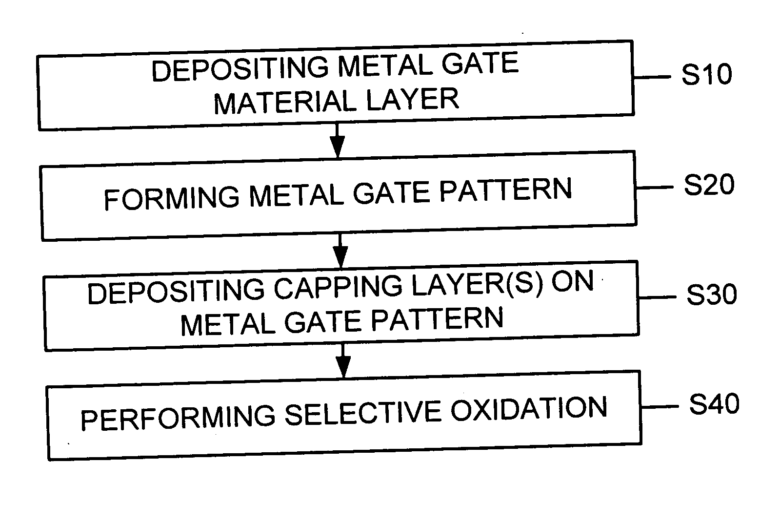
Methods of fabricating a semiconductor device having a metal gate pattern
a metal gate pattern and metal gate pattern technology, applied in the direction of semiconductor devices, radio frequency controlled devices, electrical equipment, etc., can solve the problems of reducing the effective sectional area of the gate, etching process, and damage to the surface of the silicon substrate and the sidewalls of the metal gate pattern exposed to the dry etching process
- Summary
- Abstract
- Description
- Claims
- Application Information
AI Technical Summary
Benefits of technology
Problems solved by technology
Method used
Image

Examples
Embodiment Construction
[0042] Exemplary embodiments of the present invention will now be described more fully with reference to the accompanying drawings, in which exemplary embodiments of the invention are shown. This invention may, however, be embodied in many different forms and should not be construed as being limited to the exemplary embodiments set forth herein. Rather, these exemplary embodiments are provided so that this disclosure is thorough and complete and fully conveys the concept of the invention to those skilled in the art. In the drawings, the shape of the elements may be exaggerated for clarity, and the same reference numerals in different drawings represent the same elements.
[0043] Further, it will be understood that when a layer is referred to as being "on" another layer or substrate, it can be located directly on the other layer or substrate, or intervening layers may also be present. It will also be understood that when a layer is referred to as being "directly on" another layer or su...
PUM
 Abstract
Description
Claims
Application Information