Reversible photobleachable materials based on nano-sized semiconductor particles and their optical applications

Inactive Publication Date: 2004-08-05
PIXELLIGENT TECH LLC
View PDF24 Cites 46 Cited by
  • Summary
  • Abstract
  • Description
  • Claims
  • Application Information

AI Technical Summary

Problems solved by technology

Conventional CEMs, which are based on organic polymers, however, bleach permanently.
They do not recover their original property after the incident ligh

Method used


Image

  • Reversible photobleachable materials based on nano-sized semiconductor particles and their optical applications
  • Reversible photobleachable materials based on nano-sized semiconductor particles and their optical applications
  • Reversible photobleachable materials based on nano-sized semiconductor particles and their optical applications

Examples


Embodiment Construction

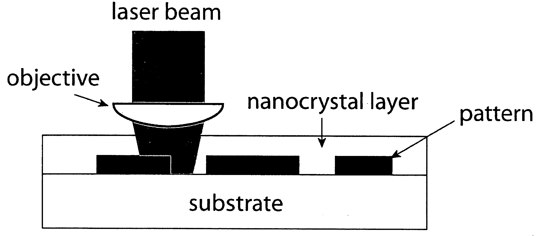
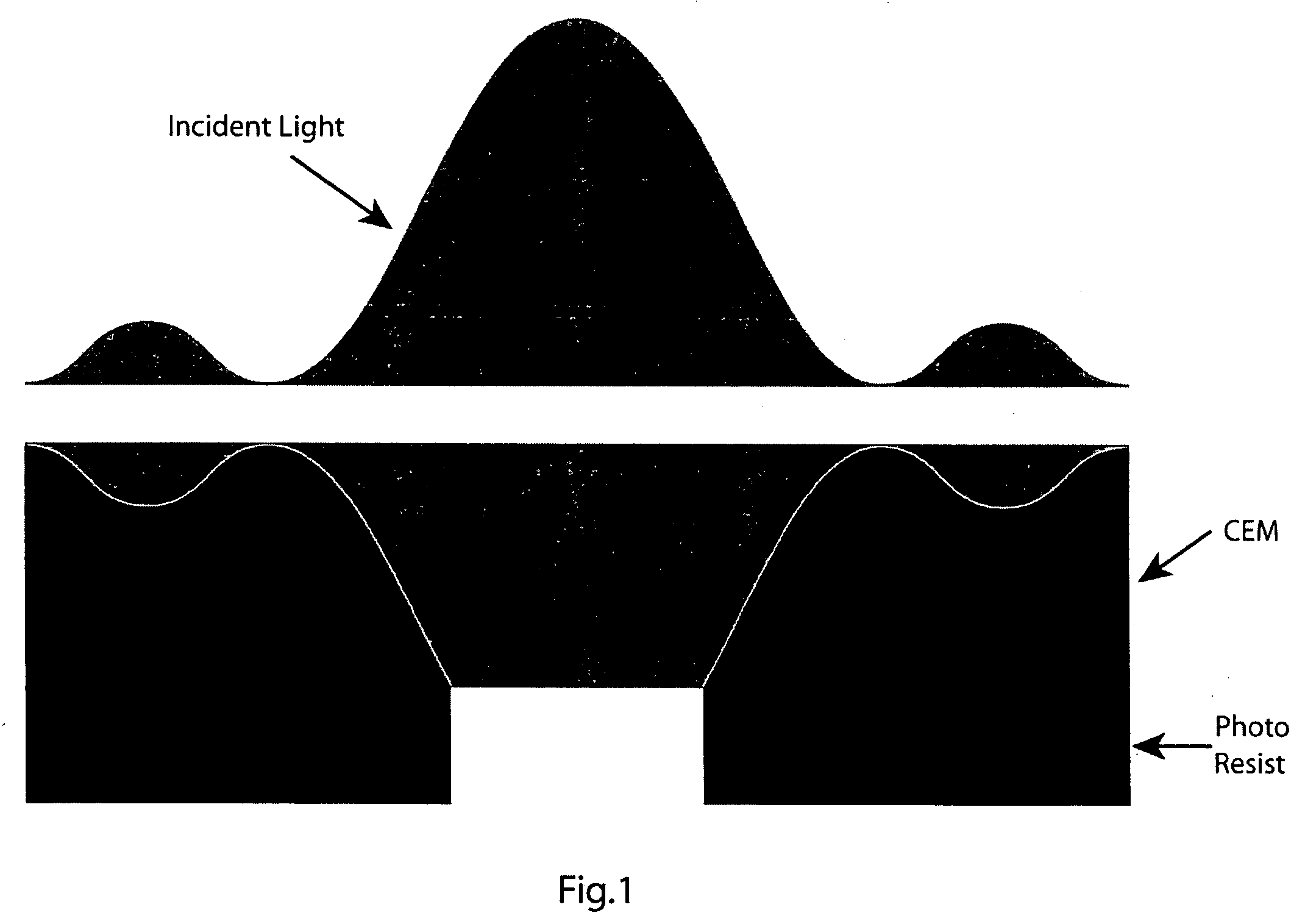
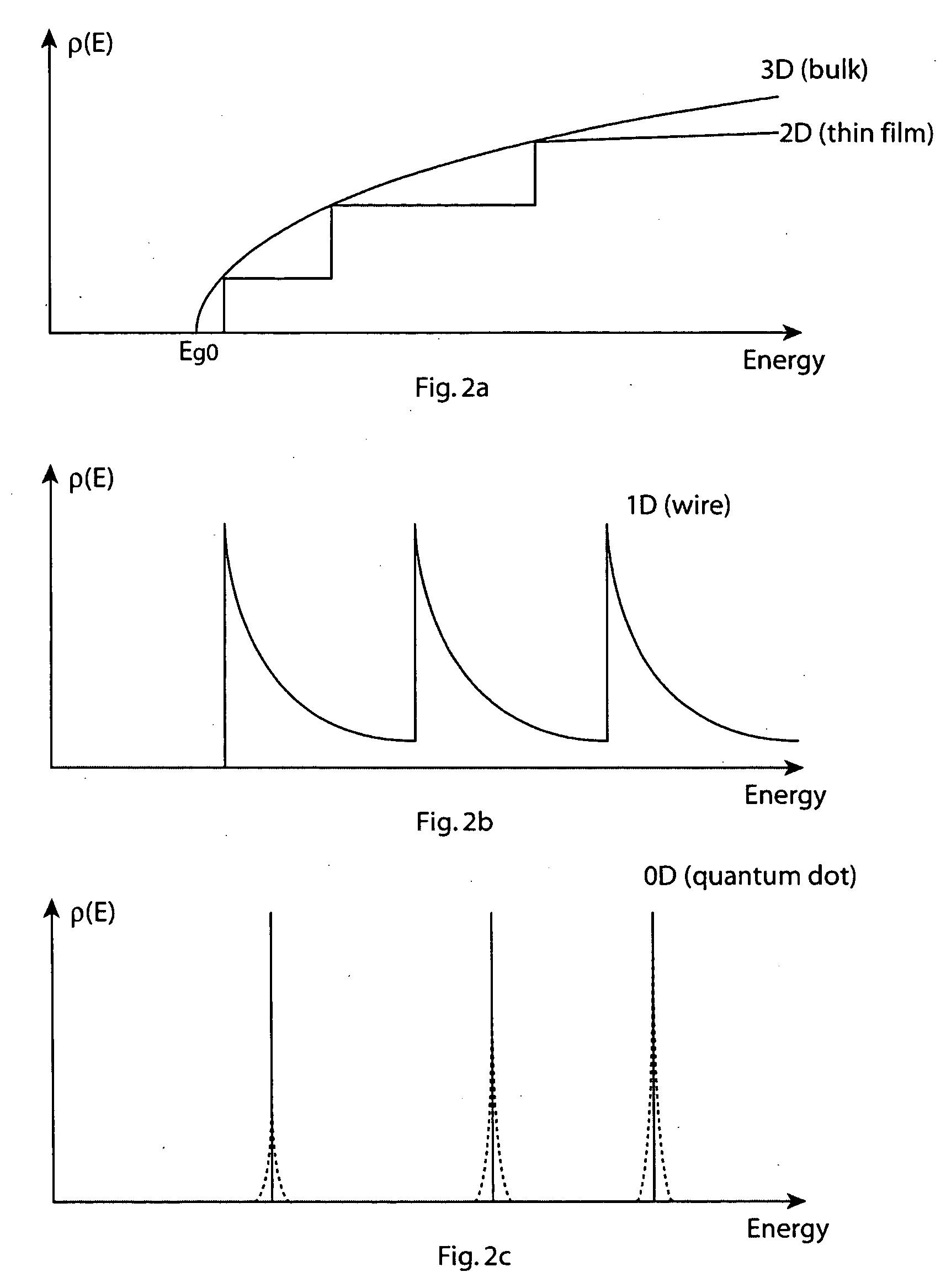
[0046] One preferred exemplary non-limiting illustrative embodiments provides a contrast enhancement material comprising semiconductor nano-sized particles. Said semiconductor may exhibit a band-gap in its electronic structure; a non-exhaustive list of said particles may include: C, Si, Ge, CuCl, CuBr, CuI, AgCl, AgBr, AgI, Ag.sub.2S, CaO, MgO, ZnO, Mg.sub.xZn.sub.1-xO, ZnS, HgS, ZnSe, CdS, CdSe, CdTe, HgTe, PbS, BN, AlN, GaN, Al.sub.xGa.sub.1-xN, GaP GaAs, GaSb, InP, InAs, In.sub.xGa.sub.1-xAs, SiC, Si.sub.1-xGe.sub.x, Si.sub.3N.sub.4, ZrN, CaF.sub.2, YF3, Al.sub.2O.sub.3, SiO.sub.2, TiO.sub.2, Cu.sub.2O, Zr.sub.2O.sub.3, ZrO.sub.2, SnO.sub.2, YSi.sub.2, GaInP.sub.2, Cd.sub.3P.sub.2, Fe.sub.2S, Cu.sub.2S, CuIn.sub.2S.sub.2, MoS.sub.2, In.sub.2S.sub.3, Bi.sub.2S.sub.3, CuIn.sub.2Se.sub.2, In.sub.2Se.sub.3, HgI.sub.2, PbI.sub.2 and their various isomers and alloys; said particles may be in spherical, cubical, rod-like, tetragonal, single or multi-wall nano-tube or other nano-scale ge...


PUM


Abstract

Semiconductor nano-particles, due to their specific physical properties, can be used as reversible photo-bleachable materials for a wide spectrum, from far infrared to deep UV. Applications include, reversible contrast enhancement layer (R-CEL) in optical lithography, lithography mask inspection and writing and optical storage technologies.

Description

CROSS-REFERENCES TO RELATED APPLICATIONS[0001] This application claims the benefit of priority from provisional application No. 60 / 431,735 filed Dec. 9, 2002, incorporated herein by reference.[0002] This application is related to U.S. Pat. No. 6,291,110 B1, entitled "Methods for Transferring a Two-Dimensional Programmable Exposure Pattern for Photolithography"; and commonly-assigned application Ser. No. ______, entitled "Programmable Photolithographic Mask Based On Semiconductor Nano-Particle Optical Modulators" filed concurrently herewith; and commonly-assigned provisional application No. 60 / 451,240, entitled "Applications of Semiconductor Nano-sized particles in photolithography system"; and commonly-assigned provisional application No. 60 / 463,626, entitled "Methods of Improving Resolution in a Photolithographic System Using Multi-image Transfer Through Layers to a Photo-resist".[0003] Not applicable.FIELD[0004] The technology herein relates to reversible photo-bleachable material...

Claims


Application Information

Patent Timeline
IPC IPC(8): G02F1/01G02F1/015G02F1/017G02F1/03G03F7/00G03F7/20H01L
CPCB82Y20/00G02F1/0126G02F1/015G02F1/01716G02F2202/36G02F2203/12Y10S430/146G03F7/70291G03F7/70383Y10T428/24802Y10T428/24893Y10S977/932G03F7/2057
Inventor CHEN, ZHIYUNFLEET, ERIN F.GONEN, SERPILCOOPER, GREGORY D.
Owner PIXELLIGENT TECH LLC
Why Eureka
Try Eureka