Method of producing silicon nanoparticles from stain-etched silicon powder

a technology of stain-etched silicon and silicon nanoparticles, which is applied in the direction of silicon compounds, silicon layered products, cellulosic plastic layered products, etc., can solve the problems of high maintenance cost of expensive equipment, inability to produce porous silicon powder, and inability to meet the requirements of high-quality production and us

Inactive Publication Date: 2004-08-26
SI DIAMOND TECH
View PDF15 Cites 95 Cited by
  • Summary
  • Abstract
  • Description
  • Claims
  • Application Information

AI Technical Summary

Problems solved by technology

This standard anodization technique is not, however, capable of producing porous silicon powder due to the inability of establishing electrical contact between particles.
Standard anodization techniques are not, however, capable of making such a porous silicon powder.
Most of these methods require either expensive equipment with high maintenance costs and / or they provide relatively low yield, considerably limiting the use of these materials for applications that require bulk quantities.
However, the product yields by this method are low.
Thus, the yield (mass efficiency) per run in this method is only about 10.sup.-5-10.sup.-6 of the mass of the precursor material (silicon wafer) which makes this approach practically unusable for mass production.
Thus, the process is limited by the presence of HNO.sub.2 at the surface of the silicon sample.

Method used


Image

  • Method of producing silicon nanoparticles from stain-etched silicon powder
  • Method of producing silicon nanoparticles from stain-etched silicon powder
  • Method of producing silicon nanoparticles from stain-etched silicon powder

Examples


Embodiment Construction

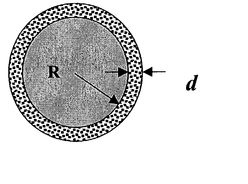
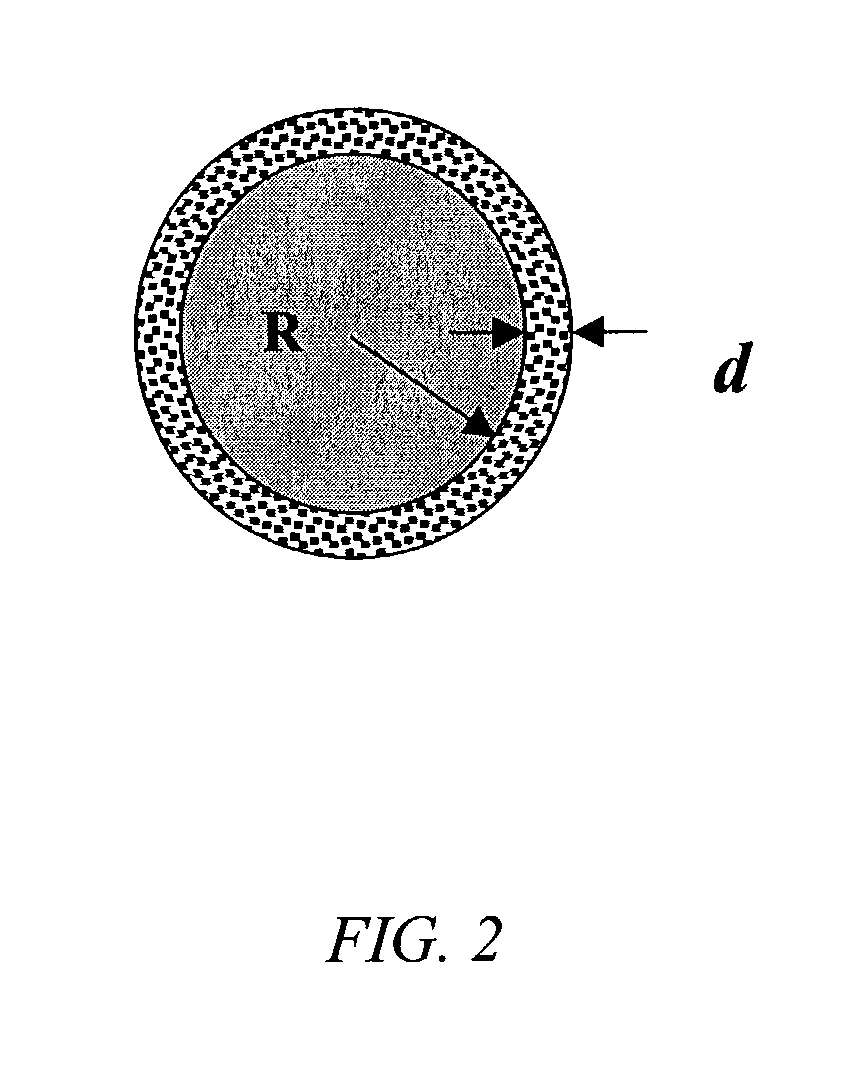
[0044] Bulk p-type silicon with a resistivity of 1-10 Ohm.multidot.cm was ground, ball milled, and sieved to produce a silicon powder comprising silicon particles with an average diameter of 100 micrometers. Approximately 0.1 grams of this silicon powder was placed in a flask with approximately 2 mL of an aqueous solution comprising 1 mL of 49 percent hydrofluoric acid and 1 mL of a 0.2 M solution of Fe(NO.sub.3).sub.3 in water. Reaction conditions comprised room temperature, in air, 30 minute duration, stirring periodically every 3-5 minutes. Evolution of NO.sub.2 was observed. The resulting porous silicon particles were then filtered, washed with water, and characterized with ultraviolet (UV) photoluminescence (PL) spectroscopy. Characterization revealed strong red-orange PL of the powder particles, indicating a porous layer on their surface.

[0045] To produce silicon nanoparticles, 0.5 grams of the porous silicon powder was redispersed in 5 mL of ethanol. This suspension was then ...


PUM

PropertyMeasurementUnit
particle diameteraaaaaaaaaa
thicknessaaaaaaaaaa

Abstract

The present invention is for a porous silicon powder comprising silicon particles wherein the outermost layers of said particles are porous. The present invention is also directed to a method of making this porous silicon powder using a stain etch method. The present invention is also directed to a method of making silicon nanoparticles from the porous silicon powders using a process of ultrasonic agitation. The present invention also includes methods of processing these silicon nanoparticles for use in a variety of applications.

Description

[0001] The present invention relates in general to materials science, and in particular, to nanostructured materials and nano-size particles, and methods for making same.BACKGROUND INFORMATION[0002] 1. Methods of Making Porous Silicon[0003] Porous silicon is a material formed on a surface of bulk silicon by forming multiple nanometer-sized pores using a chemical or electrochemical etching process. A standard electrochemical technique for making such porous silicon is the anodization of silicon. Anodization involves the application of a potential to a bulk silicon sample (e.g., a silicon wafer). For this anodization process, the wafer is immersed in an electrolyte (etching solution) which is commonly a mixture of hydrofluoric acid, water and other components. The anodization process requires a continuous and conducting sample of silicon so that it can be immersed in an electrolyte and a positive potential can be applied (Canham, Appl. Phys. Lett., 57, 1046 (1990)). This standard anod...

Claims


Application Information

Patent Timeline
Patent Type & Authority Applications(United States)
IPC IPC(8): B32B5/16C01B33/02
CPCC01B33/02C01B33/021Y10T428/2991Y10S977/90Y10T428/12479Y10T428/2993Y10T428/2982
Inventor LI, YUNJUNPAVLOVSKY, IGOR
Owner SI DIAMOND TECH
Why Eureka
Try Eureka