Light-emitting semiconductor potting composition and light-emitting semiconductor device

Active Publication Date: 2004-09-16
SHIN ETSU CHEM IND CO LTD
View PDF7 Cites 82 Cited by
  • Summary
  • Abstract
  • Description
  • Claims
  • Application Information

AI Technical Summary

Problems solved by technology

However, these transparent epoxy resins have drawbacks including poor durability to moisture due to a high percent water absorption, poor durability to light due to a low transmittance of short wavelength light, and coloring due to photo-degradation.
Regrettably, such organic compounds undergo slow curing reaction, require a long time for curing, and produce substantial residual stresses.
This necessitates the combined use of a thermoplastic resin having poor heat resistance or a hydrolyzable group-containing metal compound having poor storage stability.
In an encased light-emitting semiconductor device comprising a light-emitting member disposed in a ceramic and/or plastic housing, wherein the housing interior is filled with a silicone resin, a problem arises in a thermal shock test between -40.degree. C. and 120.degree. C., that the silicone resin separates from the ceramic or plastic housing.
Another problem arises from the fact that optical crystals of various compound semiconductors used in li

Method used


Image

  • Light-emitting semiconductor potting composition and light-emitting semiconductor device
  • Light-emitting semiconductor potting composition and light-emitting semiconductor device
  • Light-emitting semiconductor potting composition and light-emitting semiconductor device

Examples


example 1

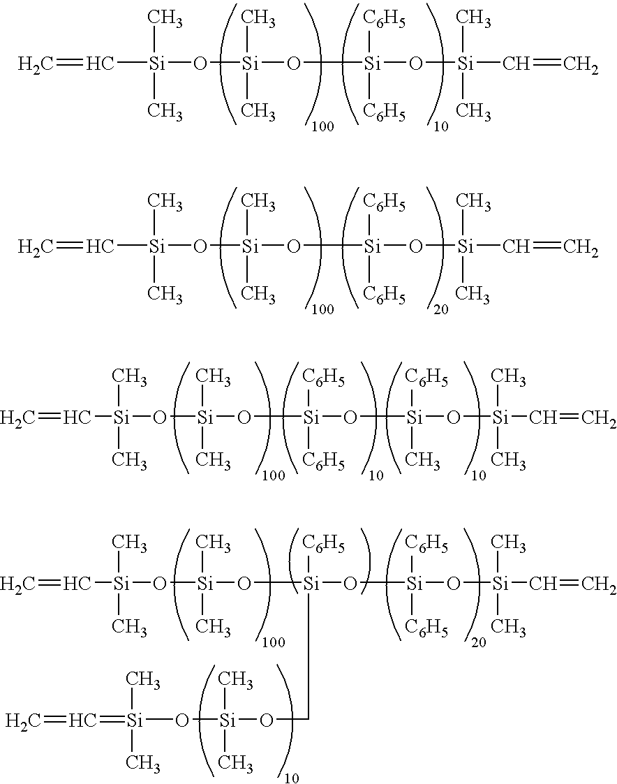
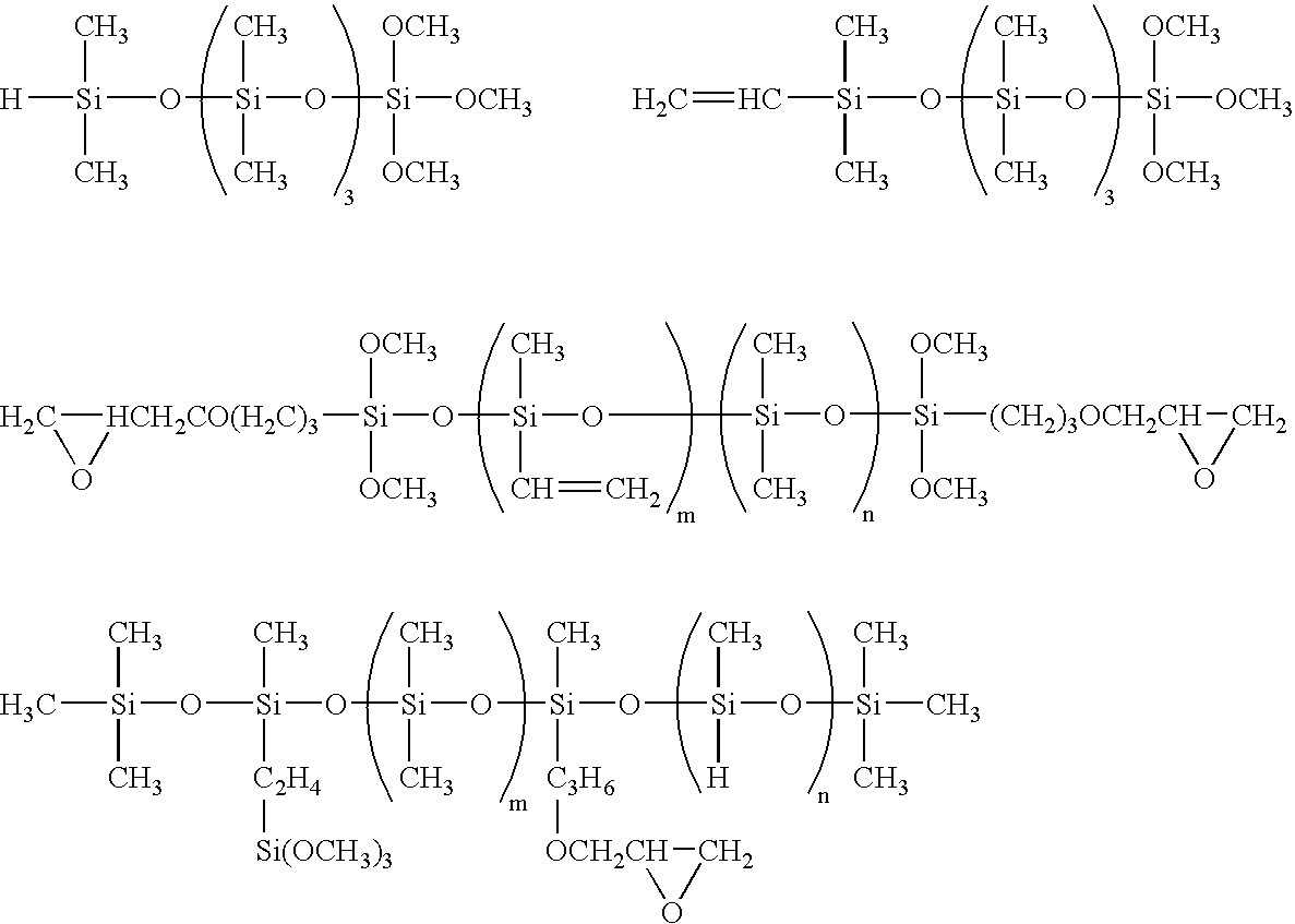
[0083] A silicone potting material was prepared by intimately mixing 100 parts of a vinyl-terminated dimethyldiphenylpolysiloxane (viscosity 3 Pa.multidot.s) having formula (I), 2.5 parts of a methylhydrogenpolysilox-ane (viscosity 15 mPa.multidot.s) having formula (II), 0.03 part of 2-ethylhexyl alcohol-modified chloroplatinic acid solution (Pt concentration 2 wt %), 0.05 part of ethynylcyclohexyl alcohol, and 2 parts of an alkoxy-containing silicone compound having formula (III). 6

[0084] The potting material cured into a silicone resin which had a Durometer type A hardness of 33 and a refractive index of 1.48 at 25.degree. C. and 589 nm. Using the potting material, a light-emitting semiconductor device was fabricated as above.

example 2

[0085] A silicone potting material was prepared by intimately mixing 100 parts of a vinyl-terminated dimethyldiphenylpolysiloxane (viscosity 5 Pa.multidot.s) having formula (IV), 7.0 parts of a methylhydrogenpolysiloxane (viscosity 90 mPa.multidot.s) having formula (V), 0.03 part of 2-ethylhexyl alcohol-modified chloroplatinic acid solution (Pt concentration 2 wt %), 0.05 part of ethynylcyclohexyl alcohol, and 3 parts of 3-methacryloxypropyltrimethoxysilane. 7

[0086] The potting material cured into a silicone resin which had a Durometer type A hardness of 24 and a refractive index of 1.45 at 25.degree. C. and 589 nm. Using the potting material, a light-emitting semiconductor device was fabricated as above.

example 3

[0087] A silicone potting material was prepared by intimately mixing 100 parts of a vinyl-terminated dimethyldiphenyl-polysiloxane (viscosity 2 Pa.multidot.s) having formula (VI), 4.1 parts of a phenylmethylhydrogenpolysiloxane (viscosity 30 mPa.multidot.s) having formula (VII), 0.03 part of 2-ethylhexyl alcohol-modified chloroplatinic acid solution (Pt concentration 2 wt %), 0.05 part of ethynylcyclohexyl alcohol, and 2 parts of an alkoxy-containing silicone compound having formula (VIII). 8

[0088] The potting material cured into a silicone resin which had a Durometer type A hardness of 62 and a refractive index of 1.53 at 25.degree. C. and 589 nm. Using the potting material, a light-emitting semiconductor device was fabricated as above.


PUM

PropertyMeasurementUnit
Temperatureaaaaaaaaaa
Fractionaaaaaaaaaa
Percent by massaaaaaaaaaa

Abstract

A potting composition comprising (A) an organopolysiloxane having a vinyl group at an end of its molecular chain, (B) an organohydrogenpolysiloxane, (C) a platinum group metal catalyst, and optionally, (D) an organosilicon compound having a silicon atom-bonded alkoxy group. The cured product of the composition has a refractive index of 1.41-1.56 at 25° C. and 589 nm (sodium D line). The composition is suited for the embedment and protection of light-emitting semiconductor members. A package in which a light-emitting semiconductor member is embedded and protected with the potting composition undergoes little discoloration and maintains a high emission efficiency in heating tests, thus offering a light-emitting semiconductor device featuring a long life and energy saving.

Description

[0001] 1. Field of the Invention[0002] This invention relates to a potting composition used for the embedment and protection of light-emitting semiconductor members and a light-emitting semiconductor device comprising a light-emitting semiconductor member embedded in the potting composition.[0003] 2. Background Art[0004] Traditional light-emitting semiconductor devices such as light-emitting diodes (LED) are lamp-type light-emitting semiconductor devices in which a light-emitting semiconductor member is disposed on a lead electrode and encapsulated with a transparent resin to a cannonball shape as shown in FIG. 3. They are recently replaced by the "surface mount" type as a result of simplification of the mounting technology. Nowadays surface mounting light-emitting semiconductor devices as shown in FIGS. 1 and 2 become the mainstream.[0005] In FIGS. 1 to 3, the device includes a housing 1 of glass fiber-reinforced epoxy resin, a light-emitting semiconductor member 2, lead electrodes...

Claims


Application Information

Patent Timeline
IPC IPC(8): C08K5/54C08L83/04G02B6/42H01L33/56
CPCC08G77/12C08G77/18H01L2224/45144H01L2224/73265H01L2224/48257H01L2224/48247H01L2224/48091H01L2224/32245H01L2224/32257H01L33/56C08L83/04C08K5/54C08G77/70C08G77/20C08L83/00H01L2924/00014H01L2924/00H01L2924/12044
Inventor YOSHINO, MASACHIKASHIOBARA, TOSHIO
Owner SHIN ETSU CHEM IND CO LTD
Why Eureka
Try Eureka