Phase interpolator and receiver

a phase interpolator and receiver technology, applied in the direction of pulse manipulation, logic circuit coupling/interface arrangement, pulse technique, etc., can solve problems such as data read error, signal voltage fluctuation, data read error,

Inactive Publication Date: 2004-09-30
KK TOSHIBA
View PDF2 Cites 88 Cited by
  • Summary
  • Abstract
  • Description
  • Claims
  • Application Information

AI Technical Summary

Problems solved by technology

If these clock signals hit the serial data 2' shift, the serial data 2' will incorrectly be read causing malfunctions in a receiver.
This will cause a data read error.
The phase interpolator according to the related art, however, causes fluctuations in the voltage of the signals 61 due to parasitic capacitance and coupling capacitance that are affected by the operation of peripheral circuits.
In addition, the voltage variations deteriorate duty ratios, making the data read circuit unable to correctly read data.

Method used


Image

  • Phase interpolator and receiver
  • Phase interpolator and receiver
  • Phase interpolator and receiver

Examples


first embodiment

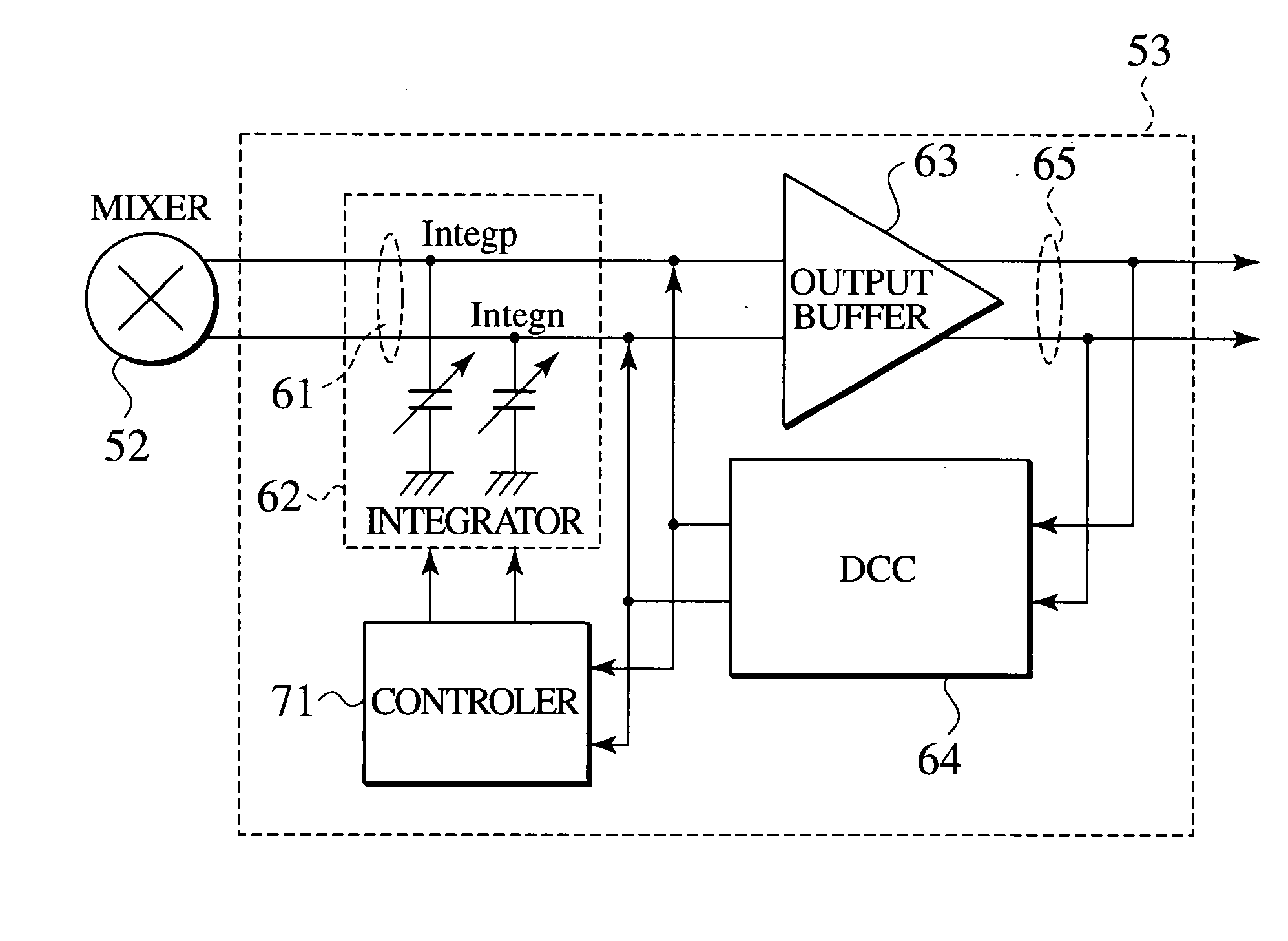
[0034] FIG. 4 is a circuit diagram showing examples of the controller 71 and integrator 62 according to the present invention. The controller 71 has an operational amplifier 21, a capacitor 12, and an inverter 13. The integrator 62 has an NMOS transistor 14a connected to one (61a) of the differential clock signals, a capacitor 15aconnected to the NMOS transistor 14a, an NMOS transistor 14bconnected to the other (61b) of the differential clock signals, and a capacitor 15b connected to the NMOS transistor 14b. The operational amplifier 21 finds a difference between the positive signal 61a or Integp and the negative signal 61b (an inverted signal due to the CML) or Integn. The operational amplifier 21 then compares the found differential voltage with a reference signal 17 or Vref. If the differential voltage is smaller than the reference signal Vref, the operational amplifier 21 provides a detected signal. Here, the capacitor 12 is able to prevent a switching of the inverter 13 upon fi...

second embodiment

[0039] FIG. 8 is a circuit diagram showing examples (71a, 62a) of the controller 71 and integrator 62 according to the present invention. Compared with FIG. 4, the controller 71a has two operational amplifiers 21a and 21bthat receive different reference signals Vref1 and Vref2, respectively. The operational amplifier 21a finds a difference between the signals Integp and Integn and compares the differential voltage with the reference signal Vref1. If the differential voltage is smaller than the reference signal Vref1, a predetermined amount of charge is accumulated in a capacitor 12a. On the other hand, the operational amplifier 21b finds a difference between the signals Integp and Integn and compares the differential voltage with the reference signal Vref2. If the differential voltage is smaller than the reference signal Vref2, a predetermined amount of charge is accumulated in a capacitor 12b. Based on these different standards, the operational amplifiers 21a and 21b turn off NMOS ...

third embodiment

[0040] FIG. 9 is a circuit diagram showing examples (71b, 62b) of the controller 71 and integrator 62 according to the present invention. The controller 71b has an operational amplifier 22a that receives the signals Integp, Integn, and Vref1, an operational amplifier 22b for receiving the signals Integp, Integn, and Vref2, a delay circuit 25 for delaying the output of the operational amplifier 22b, a flip-flop (FF) for receiving the output of the delay circuit 25 at a clock input terminal and the output of the operational amplifier 22a at an input terminal, an inverter 26 for inverting the output of the delay circuit 25, a flip-flop 24 for receiving the output of the inverter 26 at a clock input terminal and the output of the flop-flop 23 at an input terminal, and a NAND gate 27 for receiving the outputs of the flip-flops 23 and 24 and providing a NAND of the received signals. The controller 71b is an example of a counter circuit. The operational amplifier 22a receives the signals I...


PUM


Abstract

An aspect of the present invention provides a phase interpolator for adjusting a phase of differential clock signals of a receiver to a phase of a data from a transmitter that includes, an integrator configured to slew edges of differential clock signals adjusted to the phase of the data from the transmitter, a output buffer configured to amplify an output of the integrator, a duty cycle correction circuit configured to feed duty correction signals back to the adjusted differential clock signals, and a controller configured to ensure operations of an amplitude of the output buffer and a data read circuit to adjust the swings and duties of the adjusted differential clock signals.

Description

[0001] This application claims benefit of priority under 35 USC 119 based on Japanese Patent Application No. P2003-086293 filed on Mar. 26, 2003, the entire contents of which are incorporated by reference herein.[0002] 1. Field of the Invention The present invention relates generally to a phase interpolator and receiver, and more particularly, to a phase interpolator and receiver capable of ensuring operations to adjust clock phases into data phases.[0003] 2. Description of Related Art[0004] FIG. 11 is a block diagram showing a high-speed input / output (I / O) device. A transmitter 4 converts input parallel data 1 into serial data 2. In this specification, the serial data is differential pair signals from CML (current mode logic). The converted serial data 2 is transmitted to a receiver 5. The receiver 5 receives the serial data 2 and converts it into parallel data 3. The serialization of parallel data into serial data and the deserialization of serial data into parallel data are carri...

Claims


Application Information

Patent Timeline
Patent Type & Authority Applications(United States)
IPC IPC(8): H03K3/017H03K5/00H03K5/151H03K5/156H03K19/0175H03L7/06H04L7/033
CPCH03K5/151H03K5/1565H04L7/033H04L7/0025H03K2005/00045
Inventor TAKANO, MIDORI
Owner KK TOSHIBA
Why Eureka
Try Eureka