Polishing pad and semiconductor substrate manufacturing method using the polishing pad

a polishing pad and semiconductor substrate technology, applied in the direction of grinding/polishing apparatus, grinding machines, grinding/polishing tools, etc., can solve the problems of inconsistent polishing performance, excessive difficulty in practical use, and insufficient level of polishing precision and polishing efficiency to achieve the effect of high polishing precision and polishing efficiency

Inactive Publication Date: 2004-10-07
TOHO ENG CO LTD
View PDF5 Cites 14 Cited by
  • Summary
  • Abstract
  • Description
  • Claims
  • Application Information

AI Technical Summary

Benefits of technology

[0017] The present invention has been developed in order to solve the above-described problems, and it is therefore one object of this invention to provide a polishing pad of novel construction whereby the surface of a semiconductor substrate or similar material can be processed with consistently high levels of "polishing precision" and "polishing efficiency" using a CMP or similar process.
[0018] It is another object of the present invention to provide a novel semiconductor substrate fabrication method employing a polishing pad, whereby in a semiconductor fabrication process employing a suitable method such as CMP for polishing the substrate surface, the object semiconductor substrate may be fabricated with consistently high levels of "precision" and "efficiency".
[0019] It is yet another object of the present invention to provide a cutting tool for machining a groove in a polishing pad, which is capable of producing a polishing pad of novel construction pertaining to the invention, and a useful production method for the polishing pad.

Problems solved by technology

However, notwithstanding the use of these polishing pads of conventional design, it is still exceedingly difficult to achieve both "polishing precision" and "polishing efficiency" at levels adequate to meet requirements.
However, research conducted by the inventors has revealed that when grooves like those taught in Patent Document No. 4 are formed on a polishing pad surface, polishing performance, which includes both polishing efficiency and polishing precision is inconsistent.
Therefore, practical use would be extremely difficult.
It is thought that the major reason for this drawback is the variation in the width dimension of the groove in its depthwise direction.
In addition to wear produced in wafer polishing, a polishing pad is typically subjected to a conditioning process (dressing) by means of abrading the pad surface at predetermined process time intervals.
However, the grooves taught in Patent Document No. 4 unavoidably experience appreciable change in groove width due to polishing-induced wear and surface conditioning, and this is accompanied by significant variation in parameters such as the distribution of stress.
Thus, consistent polishing characteristics may be not achieved.

Method used


Image

  • Polishing pad and semiconductor substrate manufacturing method using the polishing pad
  • Polishing pad and semiconductor substrate manufacturing method using the polishing pad
  • Polishing pad and semiconductor substrate manufacturing method using the polishing pad

Examples


Embodiment Construction

[0090] There will be described in detail preferred embodiments of the invention with reference to accompanying drawings in order to further clarify the present invention.

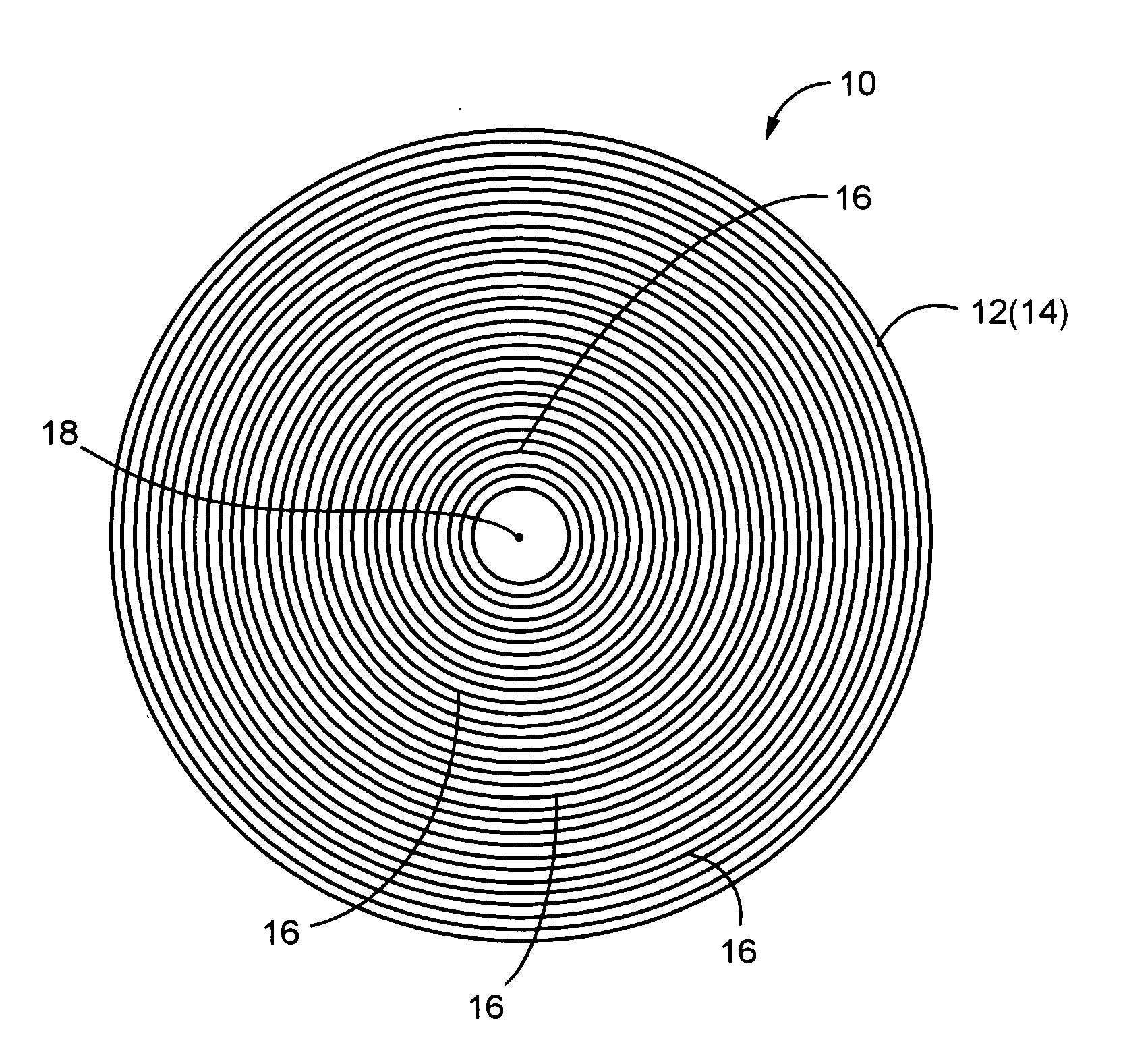
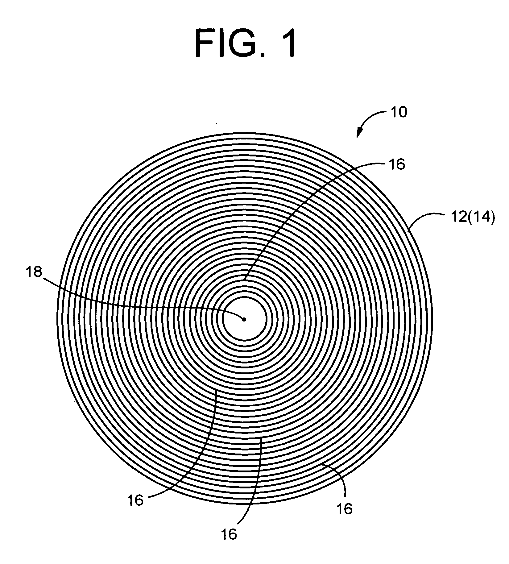
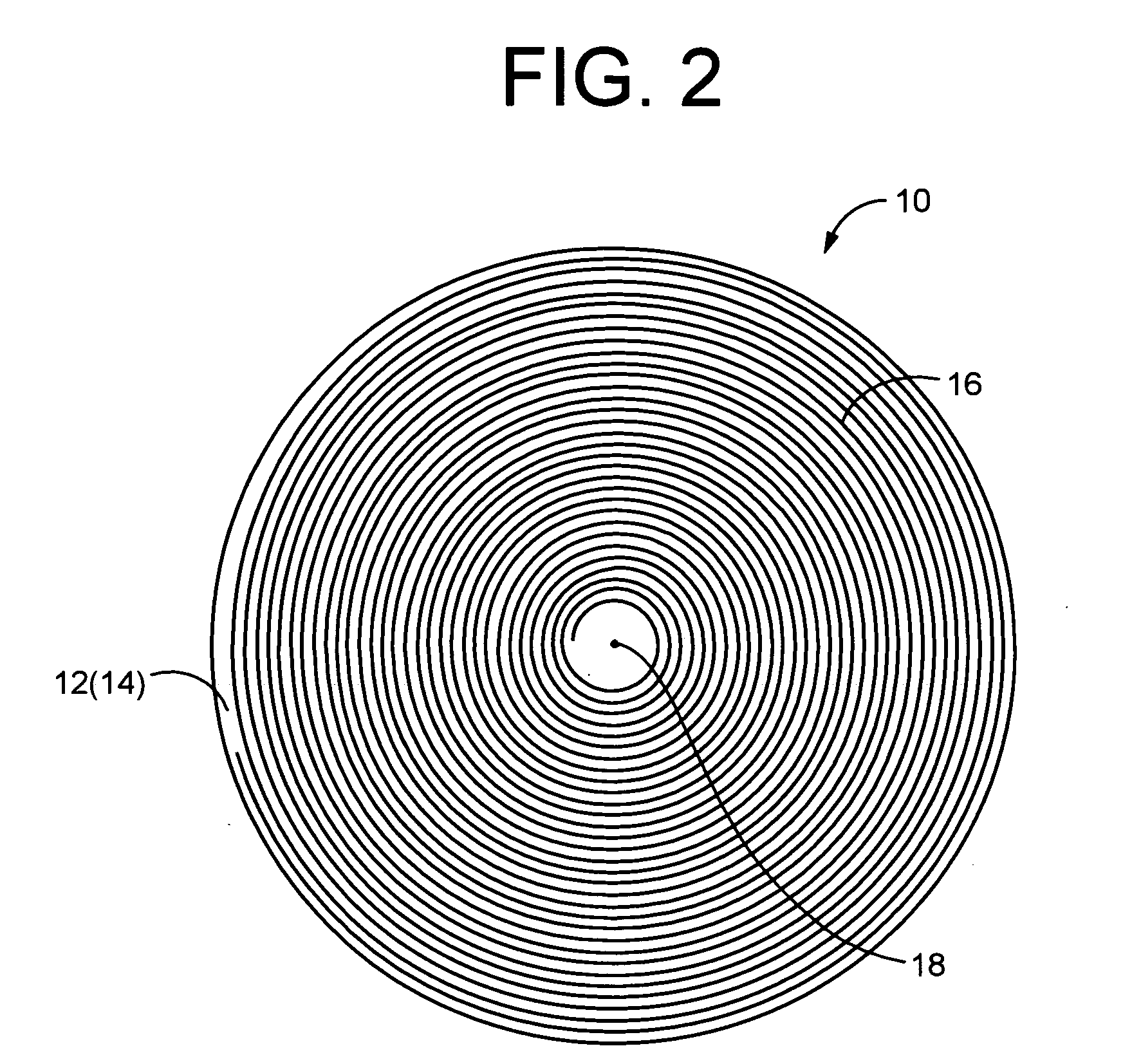
[0091] Referring first to FIG. 1, shown is a polishing pad 10 of construction according to a first embodiment of the present invention. The polishing pad 10 is constituted by a thin disk pad substrate 12 having a constant thickness dimension T overall. The pad substrate 12 is advantageously formed of rigid expanded urethane, for example. The pad thickness dimension is not particularly limited, and may be selected appropriately depending not only on the material of the pad substrate 12 but also the material of the wafer being polished, the required degree of polishing precision, and the like.

[0092] One surface 14 of the pad substrate 12, serving as a processed surface, has a groove 16 formed thereon so as to extend in a circumferential direction about an center axis 18 of the pad substrate 12, and to be open in the s...


PUM

PropertyMeasurementUnit
wedge angleaaaaaaaaaa
surface roughnessaaaaaaaaaa

Abstract

It is provided a polishing pad of novel construction capable of controlling actively and efficiently a slurry flow during polishing a surface of a semiconductor substrate, such as a wafer, thus making it possible to precisely and stably performing a desired polishing process. Onto a surface of a pad substrate 12 of synthetic resin material, formed is a groove 16 extending approximately circumferentially. An inner circumferential wall surface 20 and an outer circumferential wall surface 22 are made parallel to each other and slant with respect to a center axis 18 of the pad substrate 12.

Description

[0001] The present invention relates to a polishing pad for use in a semiconductor fabrication process, for polishing a surface of a semiconductor substrate, e.g., a semiconductor wafer or a semiconductor device. The present invention also relates to techniques associated with the polishing pad, e.g., a method of fabricating a semiconductor substrate using the polishing pad.[0002] In the process of fabricating semiconductor devices such as LSI devices, conventionally, a lamination of various kinds of thin layers including metallic layers and insulative layers are formed on a silicon wafer, for example, through various processing steps. As one major for polishing or planarizing an outer or upper most surface of the wafer to obtain a substrate surface having a high degree of planarity, chemical mechanical polishing (hereinafter referred to as "CMP") is known, wherein a thin disk-shaped polishing pad of synthetic resin material or expanded material thereof may be employed, and the poli...

Claims


Application Information

Patent Timeline
Patent Type & Authority Applications(United States)
IPC IPC(8): B24B37/20B24B37/24B24B37/26B24D3/28H01L21/302H01L21/304H01L21/461
CPCB24B37/26B24D3/28
Inventor SUZUKI, TATSUTOSHI
Owner TOHO ENG CO LTD
Why Eureka
Try Eureka