Apparatus and method for plasma enhanced monolayer processing
Inactive Publication Date: 2004-11-11
GADGIL PRASAD N
View PDF31 Cites 185 Cited by
Summary
Abstract
Description
Claims
Application Information
AI Technical Summary
This helps you quickly interpret patents by identifying the three key elements:
Problems solved by technology
Method used
Benefits of technology
Benefits of technology
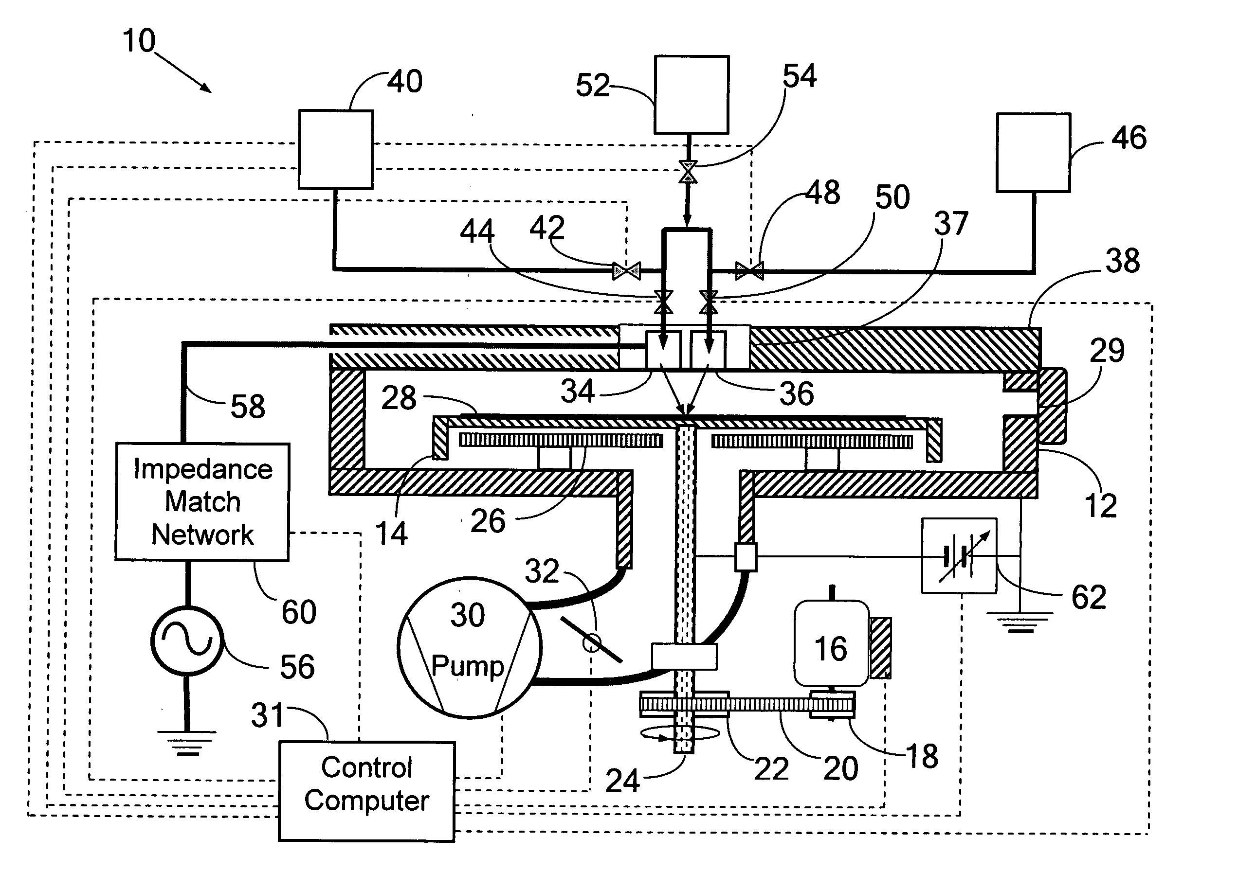
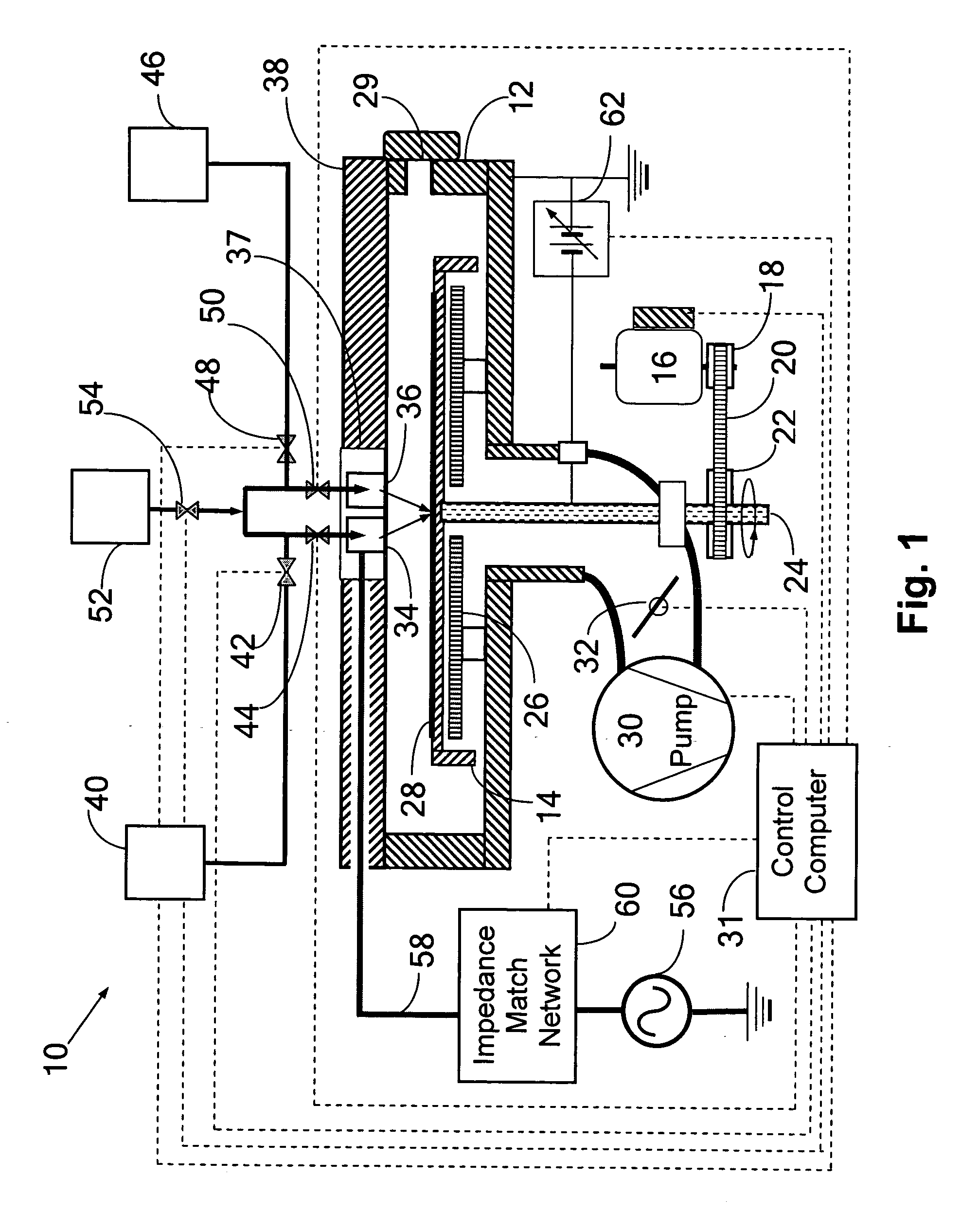
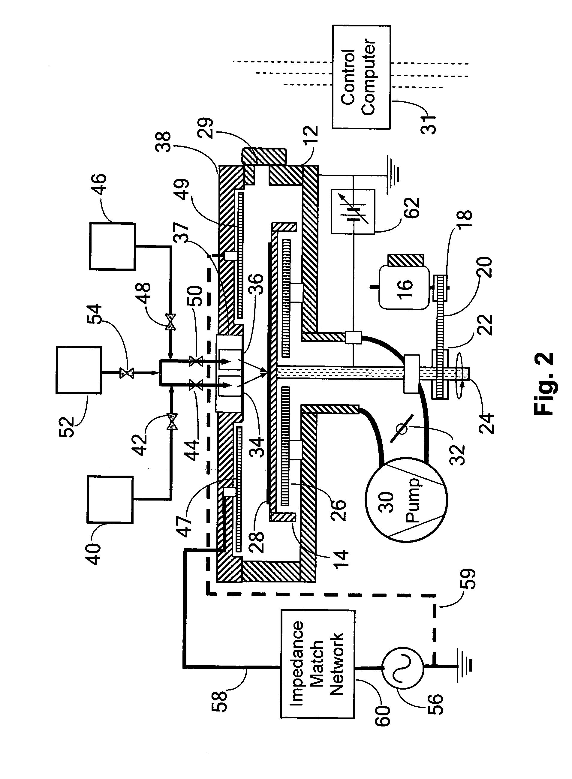
[0025] The apparatus and method of the invention: efficiently delivers process fluids, such as plasma excited gaseous species and gaseous chemical precursors, to a substrate surface; ensures rapid completion of the processing cycle without depletion of reactive gas or vapor over the substrate surface; and ensures effective and efficient separation of highly reactive gases prior to delivery to the substrate surface. The efficient delivery relies on a small reaction chamber volume and short path length of chemicals between the injectors and the substrate.
Problems solved by technology
CVD, though a high rate process, cannot deposit thin films with perfect conformality in high aspect ratio geometries; furthermore, its resolution is too coarse to deposit the extremely thin films needed for barriers, gate dielectrics and various applications.
In practice, however, ALD processes have some limitations such as: (1) reactants must be highly chemical reactive towards each other; (2) at least one reactant needs to effectively chemisorb on the substrate surface; (3) thermal activation of the reactants may lead to unacceptably high process temperatures; and (4) low-speed of ALD as compared with CVD.
Although, in principle, the technique of ALD offers a variety of advantages over the industry prevalent techniques such as CVD and PVD, at present, it is being accepted in the semiconductor industry for only a limited number of process applications.
The reasons behind the limited applications of ALD are: (a) sluggishness of typical ALD processes in the currently available apparatus, and (b) chemical processes with high reaction temperatures which can be detrimental to a variety of materials such as low-k dielectrics.
Moreover, a typical ALD apparatus cannot be used as a CVD apparatus and vice-a-versa--this necessitates separate reactor systems for thick film applications.
(a) Unstable fluid flow above the substrate and within the reactor;
(b) Depletion of reactive gas or vapor over the substrate surface which makes it impossible to achieve full surface coverage in the shortest time frame;
(c) Inadequate separation of highly reactive gases in operational space;
(d) Improper construction materials for the reaction vessel, which lead to contamination;
(e) Non-optimized path length of reactive gases within the apparatus;
(f) Non-optimized internal volume with inadequate pumping speed leading to longer residence time which results in slow ALD cycle time;
Method used
Image
Click on the blue label to locate the original text in one second.
Reading with bidirectional positioning of images and text.
Examples
example-- 2
EXAMPLE--2
[0078] Deposition of Metal Oxides: A variety of oxides of metals can be deposited by employing metal halides along with the plasma of hydrogen and oxygen mixture (alternatively water and hydrogen plasma) injected in combination with hydrogen, helium or argon as a non-condensable gas. Reaction of hydroxyl and associated reactive species in the plasma with metalhalide monolayer generates metal oxides. The metal halide can be selected with a general formula MX.sub.n where, M: Al, Si, In, Sn, Pb, Ba, Sr, Ni, Ti, Ta, Zr, Nb, Hf, Mo, W, Fe, Co, Ni, Co, and Cu and other transition metals. Whereas, X=F, Cl, Br or 1.
example-- 3
EXAMPLE--3
[0079] Deposition of Metal Nitrides: A variety of oxides of corresponding metals can be deposited by employing metal halides through the first injector with hydrogen as a non-condensable gas and ammonia as the second chemical precursor. Alternately, NH.sub.x species can be conveniently generated by pulsing N.sub.2 in hydrogen plasma. The overall reaction can be described as:
[0082] Examples of M are, but not limited to, Al, Ti, Ta, Zr, Nb, Hf, Mo, W, Co, Ni, Cu and X is selected from F, Cl, Br or 1.
example-- 4
EXAMPLE--4
[0083] Deposition of Metal Carbides: Metal carbides are deposited by employing hydrogen as a non-condensable gas with methyl halide (CH.sub.3X, X=F, Cl, Br and 1) as a carbon precursor and metal halides as the metal precursor in hydrogen plasma. Some examples of metal halides are: SiCl.sub.4, TiCl.sub.4, WF.sub.6, MoF.sub.6, TaCl.sub.5, ZrCl.sub.5 etc. The mechanism of deposition of carbides can be described as:
PUM
Property
Measurement
Unit
Size
aaaaa
aaaaa
Shape
aaaaa
aaaaa
Electric potential / voltage
aaaaa
aaaaa
Abstract
An apparatus and method for plasma enhanced monolayer (PEM) processing, wherein excited species from a non-condensable gas plasma are delivered to a substrate surface during the reaction of a chemical precursor with a previously chemisorbed monolayer on the substrate surface; the excited species lower the activation energy of the monolayer formation reaction and also modulate the film properties. In preferred embodiments a process reactor has linear injectors arranged diametrically above a substrate and reactive gases are sequentially injected onto the substrate surface while it is being rotated. The reactor can be operated in pulse precursor and pulsed plasma, constant precursor and constant plasmamodes, or a combination thereof.
Description
[0001] This application is a continuation-in-part of U.S. application Ser. No. 10 / 019,244 filed on May 20, 2002 which is based on the International Application No. PCT / US 00 / 17202 filed on Jun. 23, 2000 with priority date of Jun. 24, 1999.[0002] 1. Field of the Invention[0003] The present invention relates to manufacturing of semiconductor devices, particularly to an apparatus and method for delivery of reactive chemical precursors to the surface of a substrate which is to be treated or coated, e.g., with a synchronized pulsed plasma processing apparatus for processing of thin films on substrates, e.g., in semiconductor device fabrication or in a similar field.[0004] 2. Description of the Related Art[0005] Manufacturing of advanced integrated circuits (ICs) in the microelectronic industry is accomplished through numerous and repetitive steps of deposition, patterning, and etching of thin films on the surface of silicon wafers. An extremely complex, monolithic and three-dimensional s...
Claims
Application Information
Patent Timeline
Application Date:The date an application was filed.
Publication Date:The date a patent or application was officially published.
First Publication Date:The earliest publication date of a patent with the same application number.
Issue Date:Publication date of the patent grant document.
PCT Entry Date:The Entry date of PCT National Phase.
Estimated Expiry Date:The statutory expiry date of a patent right according to the Patent Law, and it is the longest term of protection that the patent right can achieve without the termination of the patent right due to other reasons(Term extension factor has been taken into account ).
Invalid Date:Actual expiry date is based on effective date or publication date of legal transaction data of invalid patent.

