Nitride semiconductor laser device and manufacturing method therefor

a laser device and semiconductor technology, applied in the direction of semiconductor lasers, polycrystalline material growth, crystal growth process, etc., can solve the problems of accelerated degradation of end faces, damage to active layers, etc., to reduce dislocation density, avoid cracking, and reduce dislocation density

Inactive Publication Date: 2004-12-02
AMMONO SP Z O O (PL)
View PDF43 Cites 107 Cited by
  • Summary
  • Abstract
  • Description
  • Claims
  • Application Information

AI Technical Summary

Benefits of technology

[0011] According to the present invention, AMMONO method may be applied to form the single crystal Al.sub.xGa.sub.1-xN (0.ltoreq.x.ltoreq.1) at a low temperature. Using of AMMONO method, under a supercritical condition of ammonia, the single crystal Al.sub.xGa.sub.1-xN (0.ltoreq.x.ltoreq.1) layer can be grown on a predetermined seed face, i.e. an end face of the resonator in the laser device according to this invention, and the end face film of single crystal can be formed at a temperature 900.degree. C. or less, preferably 600.degree. C. or less, more preferably 500.degree. C. or less. In the AMMONO method, the end face film can be usually influenced by the autoclave composition and can contain at least one element selected from the group consisting of Ni, Cr, Co, Ti, Fe, Al, Si and Mn. The AMMONO method is characterized in that the end face film includes at least one element, used as a mineralizer, from Group No. 1 (IUPAC. 1989) element, Li, K, Na or Cs. According to the present invention, light from the nitride semiconductor laser device can not be absorbed on the end face film, which leads no heat absorption on the light emitting end face and COD generation can be reduced in the nitride semiconductor laser device at the power output 100 mW or more.
[0047] To improve the smoothing effect of the end face film 5, it is recommended that the ratio of Al be lower. Nevertheless, according to the present invention, to improve the operation of the window structure, a small content of Al is desirable. Therefore Al content can be zero, and the end face film 5 should be composed of Al.sub.xGa.sub.1-xN where preferably 0.ltoreq.x.ltoreq.0.3, and more preferably 0.ltoreq.x.ltoreq.0.15.

Problems solved by technology

Such high temperature causes damage to the active layer containing In.
Moreover, as a result of coloring of amorphous, light absorption and heating on end faces will occur, which consequently leads to accelerated degradation of end faces.

Method used


Image

  • Nitride semiconductor laser device and manufacturing method therefor
  • Nitride semiconductor laser device and manufacturing method therefor
  • Nitride semiconductor laser device and manufacturing method therefor

Examples


example 2

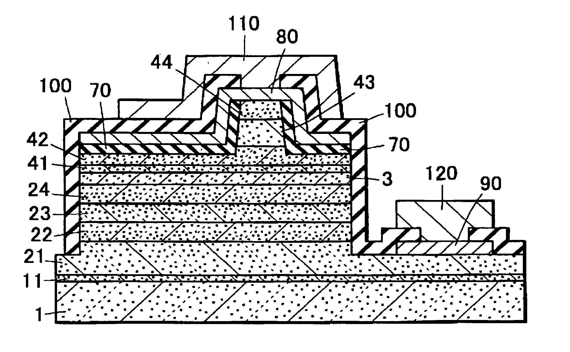
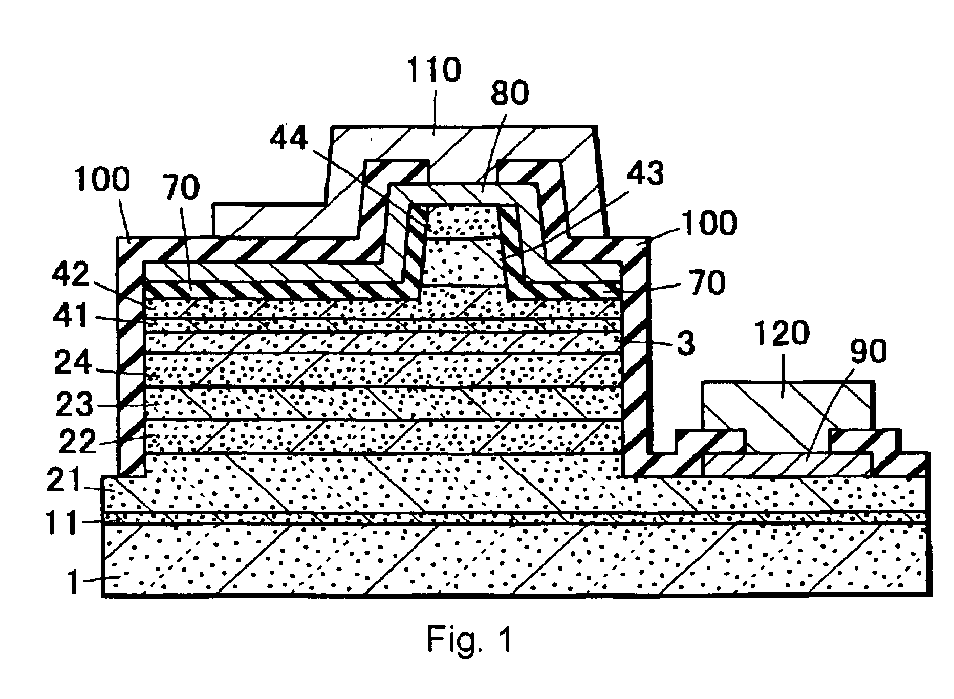
[0071] A single crystal GaN end face film of 1 .mu.m thickness is grown on the only one light emitting end face on the stripe part, whereas other stages of production of nitride semiconductor laser device are carried out similarly as in Example 1.

[0072] Each laser device manufactured in this way is equipped with a heat sink and the laser oscillation is carried out. Prolonged laser lifetime in continuous oscillation mode is expected--with threshold current density: 2.0 kA / cm.sup.2, power output: 100 mW and 405 nm oscillation wavelength--similar as in Example 1.

example 3

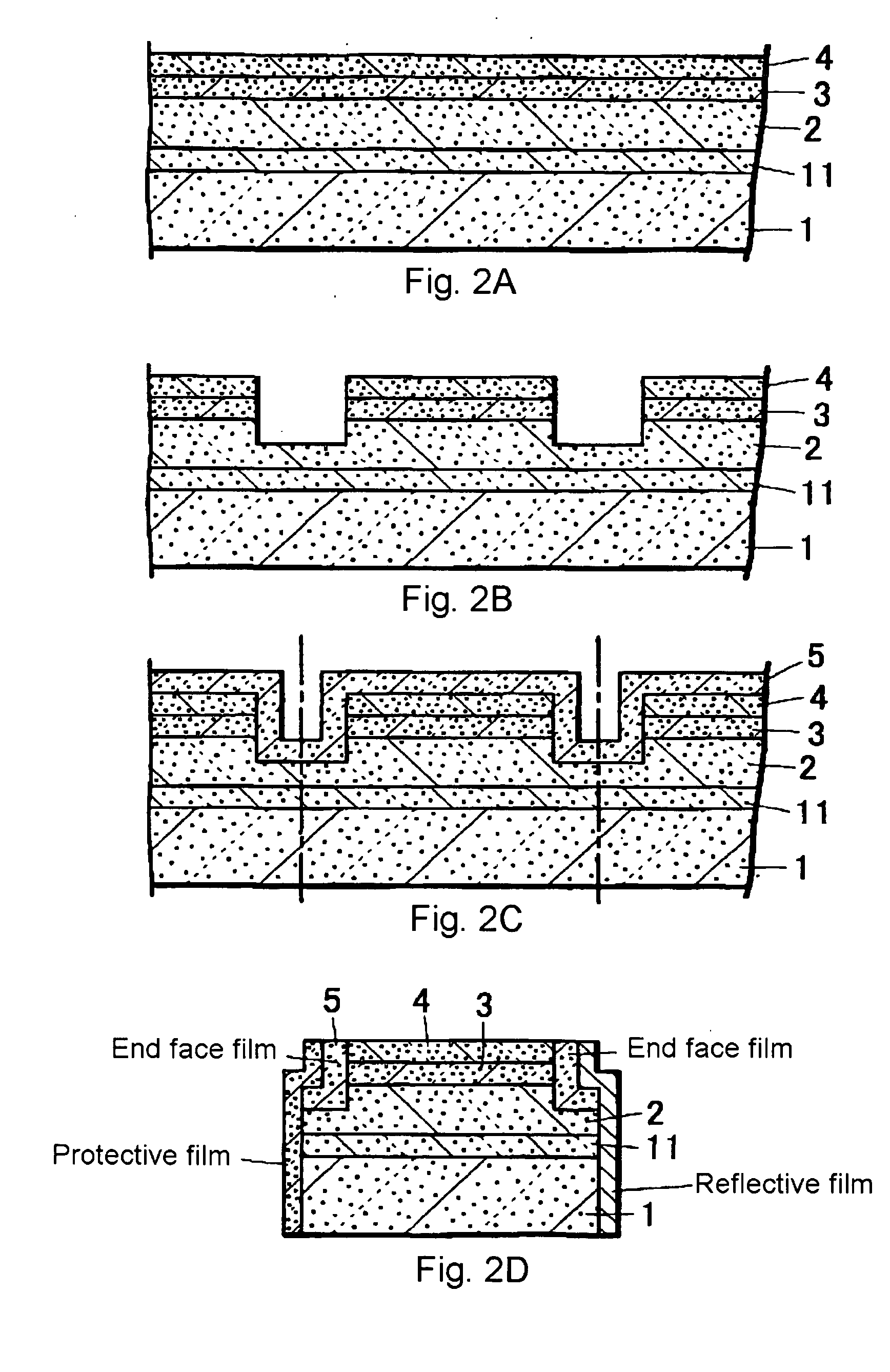
[0073] After the buffer layer is formed on a sapphire substrate, a 100 .mu.m thickness GaN layer is deposited by the HVPE method. Next, as in Example 1, the n-type nitride semiconductor layer, the active layer and the p-type nitride semiconductor layer are formed. Then the sapphire substrate is removed and consequently a homogenous GaN substrate is obtained. In the other stages, as in Example 1, after the formation of an end face of the resonator, single crystal GaN of 100 .ANG. thickness is formed on the end face film in the supercritical ammonia. Nitride semiconductor laser device thus obtained is expected to have the similar effect as in Example 1.

example 4

[0074] After the buffer layer is formed on a sapphire substrate, a 100 .mu.m thickness GaN is deposited through ELO layer by HVPE method. Next, as in Example 1, the n-type nitride semiconductor layer, the active layer and the p-type nitride semiconductor layer are formed. Then the sapphire substrate is removed and consequently a nitride semiconductor laser device is obtained on a homogenous GaN substrate. By using the cleavage property of the homogenous GaN substrate, cleavage is carried out to obtain the growth face for the end face film. Next, the single crystal GaN of 1 .mu.m thickness as an end face film is formed on the light emitting end face in the supercritical ammonia. In the other stages, as in Example 1, after the formation of an end face of a resonator, nitride semiconductor laser devices are formed. Nitride semiconductor laser device thus obtained is expected to have the similar effect as in Example 1.


PUM

PropertyMeasurementUnit
thicknessaaaaaaaaaa
temperatureaaaaaaaaaa

Abstract

The object of this invention is to provide a high-output type nitride semiconductor laser device comprising a pair of end faces of a resonator. The nitride semiconductor laser device comprises an n-type nitride semiconductor layer or layers, a p-type nitride semiconductor layer or layers and a resonator, provided with an active layer comprising nitride semiconductor containing In therebetween, wherein at least light emitting end face of the resonator is covered with an end face film of single crystal AlxGa1-xN (0<=x<=1) formed at a low temperature not causing damage to the active layer comprising nitride semiconductor containing In.

Description

[0001] This invention relates to a nitride semiconductor laser device provided with an end face film of single crystal Al.sub.xGa.sub.1-xN (0.ltoreq.x.ltoreq.1) covering an end face or faces of the resonator.[0002] In the so-far used semiconductor laser devices made from GaAs based semiconductors, extension of the lifetime of a laser device is achieved due to formation of a window structure where a protective film is formed on end faces of a resonator in the laser device. Similarly, in a nitride semiconductor of a nitride semiconductor laser device, end faces of a resonator are obtained by means of RIE (Reactive Ion Etching) or cleavage, which makes energy gap of end faces narrow, resulting in absorption of light and heat generation on the end faces that leads to impairment of the lifetime in making high-output type, i.e. over 100 mW, lasers. Therefore, it has been suggested that the window structure in nitride semiconductor laser device should be obtained by way of forming a protec...

Claims


Application Information

Patent Timeline
Patent Type & Authority Applications(United States)
IPC IPC(8): C30B7/00C30B7/10C30B9/00C30B29/40H01L21/318H01S5/00H01S5/02H01S5/028H01S5/16H01S5/22H01S5/32H01S5/323H01S5/343
CPCB82Y20/00C30B7/005C30B9/00C30B29/403C30B29/406H01S5/021H01S5/0213H01S5/0218H01S5/0281H01S5/164H01S5/22H01S5/3202H01S5/32341H01S5/34333H01S2304/12C30B7/10H01S5/32025H01S5/30
Inventor DWILINSKI, ROBERTDORADZINSKI, ROMANGARCZYNSKI, JERZYSIERZPUTOWSKI, LESZEKKANBARA, YASUO
Owner AMMONO SP Z O O (PL)
Why Eureka
Try Eureka