
Method of and apparatus for processing substrates

a technology of substrates and apparatuses, applied in the field of semiconductor devices, can solve the problems of organic substance, large amount of fluorine (f) atoms, and easy left-over residual substance after liquid evaporated

Inactive Publication Date: 2004-12-16
TOKYO ELECTRON LTD
View PDF10 Cites 10 Cited by
  • Summary
  • Abstract
  • Description
  • Claims
  • Application Information

AI Technical Summary

Benefits of technology

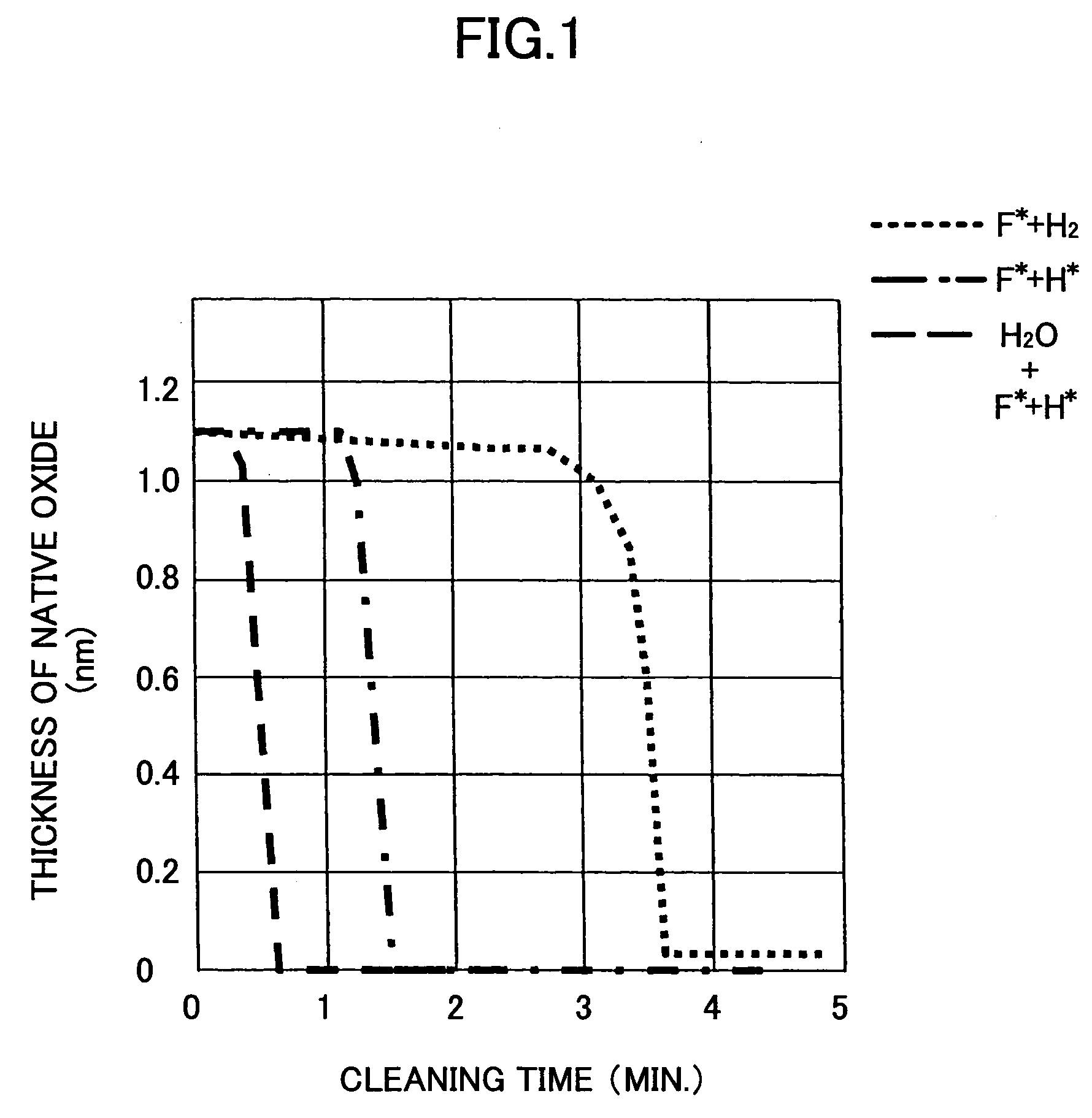
[0014] Another and more specific object of the present invention is to provide a method of and an apparatus for removing native oxide in which no residual substance is left and the amount of absorbed fluorine is minimized.

Problems solved by technology

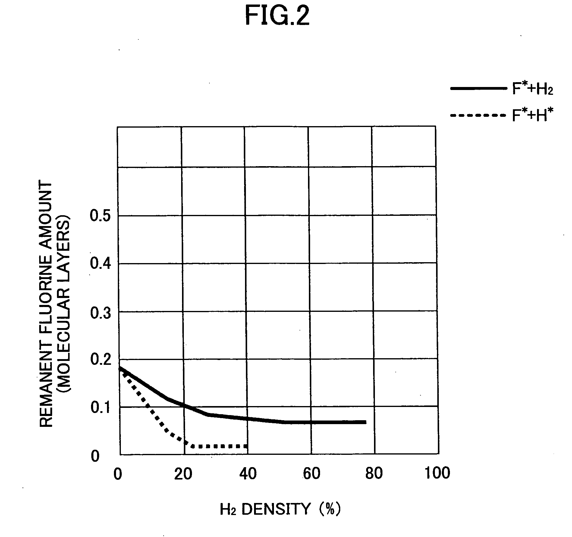
One of the problems of the conventional methods is that a large amount of fluorine (F) atoms remain on the surface of the processed silicon substrate after processing, and residual substance is easily left after the liquid evaporates.
Another problem of the conventional methods is caused by organic substance absorbed on the surface of the silicon substrate that is difficult to remove before the removal of native oxide.
However, a large amount of fluorine (F) atoms are absorbed on the surface of the silicon substrate.

Method used


Image

  • Method of and apparatus for processing substrates
  • Method of and apparatus for processing substrates
  • Method of and apparatus for processing substrates

Examples


first embodiment

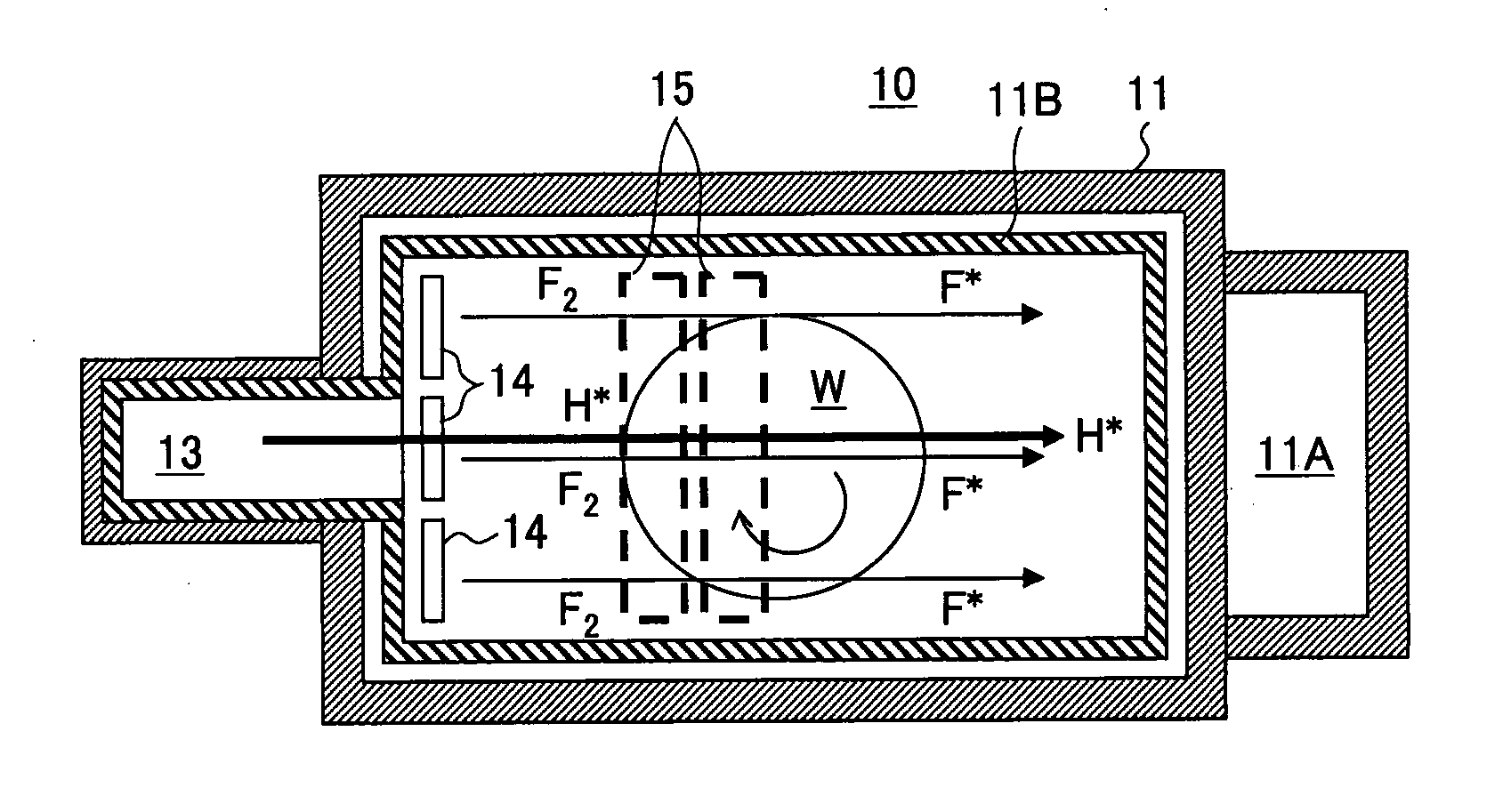
[0076] FIGS. 3A and 3B are a top view and a sectional view, respectively, showing an apparatus 10 for processing a substrate according to the present invention.

[0077] Referring to FIGS. 3A and 3B, the apparatus 10 for processing a substrate has a processing vessel 11 that is provided with a vacuation port 11A at an end thereof. A mount 12 that retains a substrate W that is to be processed is provided in the processing vessel 11.

[0078] An inner processing vessel 11B made of quartz glass is formed inside the processing vessel 11. A remote plasma source 13 is provided at another end of the processing vessel 11.

[0079] Hydrogen gas is provided to the remote plasma source 13 together with inert gas such as argon Ar. Hydrogen radicals H* are generated by exciting the hydrogen gas at a high frequency of 400 kHz, for example. The generated hydrogen radicals H* flow in the quartz processing vessel 11B along the surface of the substrate W on the mount 12 to the vacuation port.

[0080] The appara...

second embodiment

[0096] FIG. 6 is a schematic diagram showing a gas providing system used for an apparatus for processing a substrate according to a second embodiment of the present invention. The apparatus for processing a substrate according to this embodiment is substantially identical to the apparatus 10 for processing a substrate described above, and its description is omitted. In FIG. 6, elements that have been described above are referred to by the same reference numerals, and their description is omitted.

[0097] Referring to FIG. 6, according to this embodiment, a line 14m for providing water vapor (H.sub.2O) including valves 14M and 14N and a mass flow controller 140 is added to the gas providing system connected to the processing gas port 14.

[0098] When native oxide is removed by hydrogen radicals H* and fluorine radicals F*, water vapor is provided to the processing vessel 11 as catalyst via the line 14m of the gas providing system shown in FIG. 6. The water vapor promotes the process of r...

third embodiment

[0099] FIG. 7 is a flow chart showing a process for removing native oxide according to a third embodiment of the present invention that is performed by the apparatus 10 for processing a substrate shown in FIG. 3 and the gas providing system shown in FIG. 6.

[0100] Referring to FIG. 7, in step S11, Ar gas is introduced into the quartz processing vessel 11B via the line 14a, for example. Pressure in the quartz processing vessel 11B is maintained at 133 Pa, and temperature of the substrate W is maintained at 300.degree. C.

[0101] In step S12, pressure in the processing vessel 11B is set in a range of 13.3 Pa--about 4 kPa thereby to generate plasma in the remote plasma source 13. Ar gas and hydrogen gas are provided to the remote plasma source 13 via the line 14a and the line 14b, respectively. The flow of Ar gas is maintained at 500 SCCM through 1000 SCCM, and the flow of hydrogen gas is maintained at 100 SCCM. A 1 kW, 400 kHz electric power is provided to the remote plasma source 13 the...


PUM

PropertyMeasurementUnit
thickaaaaaaaaaa
thicknessaaaaaaaaaa
frequencyaaaaaaaaaa

Abstract

A dry cleaning process for removing native oxide at improved efficiency is disclosed. The dry cleaning process minimizes the amount of fluorine atoms absorbed on the surface of a processed substrate. Fluorine radicals are provided to the substrate together with hydrogen radicals. The substrate is processed by the reaction of the fluorine radicals and the hydrogen radicals.

Description

[0001] 1. Field of the Invention[0002] The present invention generally relates to the fabrication of a semiconductor device, and particularly, to a so-called pre-cleaning process for removing native oxide formed on the surface of a silicon substrate.[0003] 2. Description of the Related Art[0004] Native oxide formed on the surface of a silicon substrate needs to be removed before various processes such as an insulation film forming process and an epitaxial process on the silicon substrate. The native oxide includes, for example, an oxide film formed due to the atmospheric oxidation of hydrophobic silicon surface formed by cleaning the silicon surface with diluted fluorine acid and an oxide film unintentionally formed in oxidation processing, dilution processing, and CVD processing, for example, even at a low temperature.[0005] The native oxide needs to be completely removed in the recent fabrication of super fine semiconductor devices in which, for example, a high dielectric gate ins...

Claims


Application Information

Patent Timeline
Patent Type & Authority Applications(United States)
IPC IPC(8): H01L21/3065B08B7/00H01L21/00H01L21/304H01L21/306
CPCB08B7/0035H01J37/32357H01L21/02046H01L21/67028
Inventor SHINRIKI, HIROSHIAOYAMA, SHINTARO
Owner TOKYO ELECTRON LTD
Learn More