Energy conversion and storage films and devices by physical vapor deposition of titanium and titanium oxides and sub-oxides
a technology of energy conversion and storage films, applied in vacuum evaporation coatings, sputtering coatings, coatings, etc., can solve the problems of poor insulation properties, difficult amorphous titania deposited, and not utilized commercially for titanium oxide layers
- Summary
- Abstract
- Description
- Claims
- Application Information
AI Technical Summary
Problems solved by technology
Method used
Image
Examples
examples 2
Deposition of TiO2 on Ti-Ti4O7 film Stack
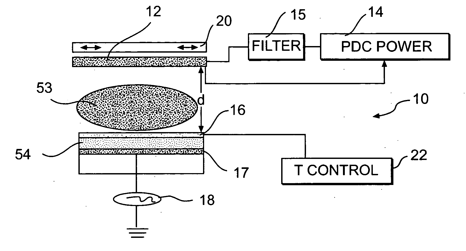
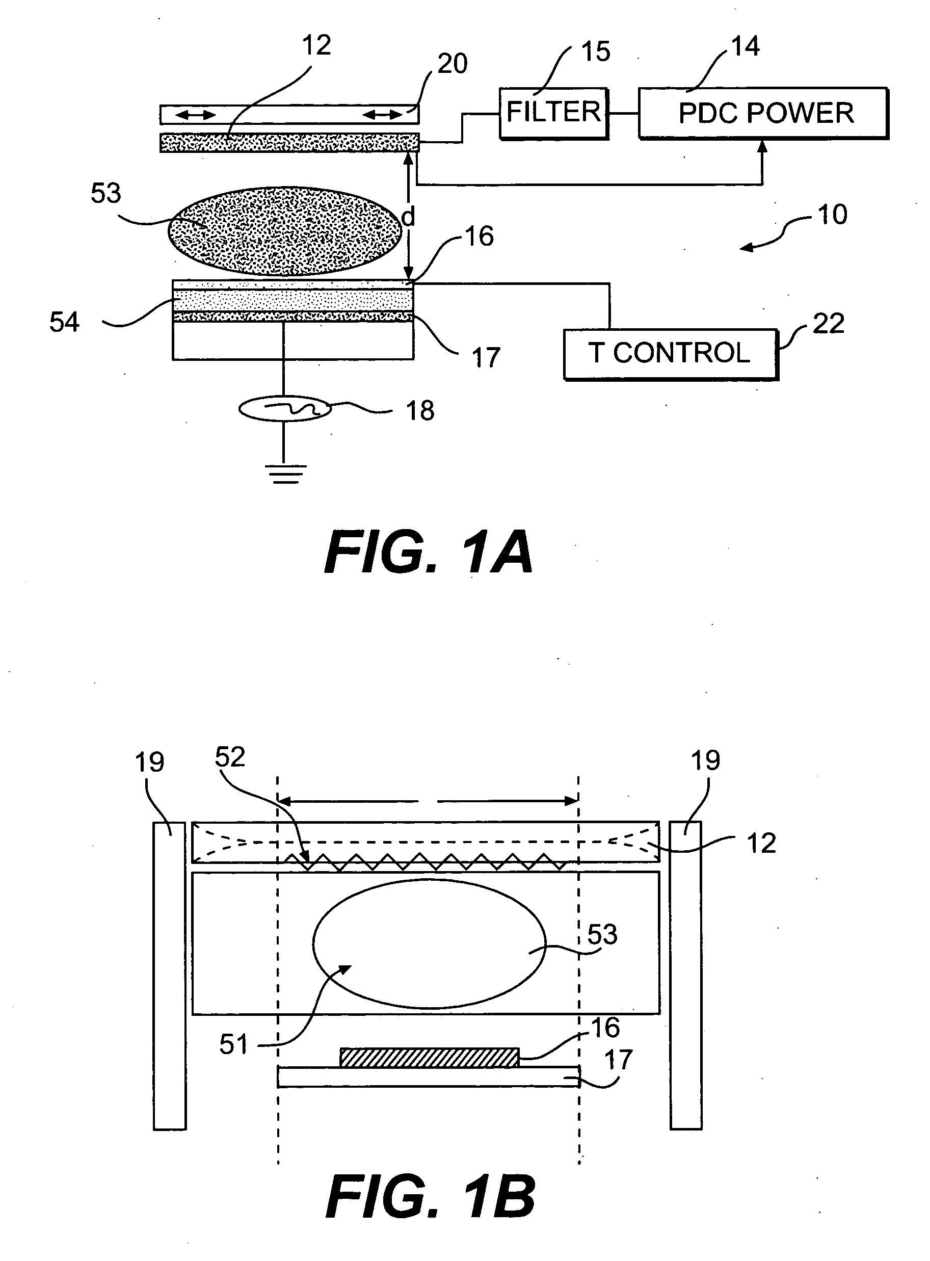
[0068] In this example, TiO.sub.2 films were deposited using a 2 MHz RF biased, Pulse DC scanning magnetron PVD process as was previously described in U.S. application Ser. No. 10 / 101,341. The substrate size can be up to 600.times.720 mm.sup.2. The target was a .about.7 mm thick, .about.630.times.750 mm.sup.2 Ti plate of 99.9% purity. A pulsed DC generator, or PDC power supply from Advanced Energy (Pinnacle Plus) was used as the target power supply. The pulsing frequency can be varied from 0-350 KHz. Reversed duty cycle can be varied from 1.3 .mu.s to 5 .mu.s depending on the pulsing frequency. An ENI RF generator and ENI Impedance matching unit were used for the substrate bias. A 100 W with a 2 MHz RF generator, which can be an EFI supply, was utilized. The chamber base pressure was kept below 2.times.10.sup.-7 Torr. The substrate temperature was below 200.degree. C. during deposition.
[0069] A systematic DOE (design of experiments) were carr...
example 3
Deposition of TiO2 on Ti-TiO.sub.x (x<2) Film Stack
[0073] A layer of TiO.sub.2 was deposited on a titanium coated substrate. About 2000 .ANG. of Ti metal was deposited at 7 KW of PDC target power, with Ar flow of 100 sccm and bias power of 200 W. After Ti deposition, TiO.sub.2 was deposited in the same chamber without-oxide burn in. This process resulted in a Ti-TiO.sub.y-TiO.sub.2 (y<2) film stack. The k value of a 200 .ANG. film was as high as 60.
[0074] FIGS. 9A and 9B illustrate an SEM cross-section of a Ti.sub.4O.sub.7 Ebonex.TM. target (FIG. 9A) and an SEM cross section of the Ti.sub.4O.sub.6.8 layer (FIG. 9B) deposited from the Ebonex.TM. target according to the present invention. The deposited film shows smooth deposition of the layer. The Ebonex.TM. target shown in FIG. 9A shows an open porousity material with high roughness. The deposited layer shown in FIG. 9B, however, shows a highly dense layer with a smooth surface condition.
[0075] Table I shows the effects of the diele...
PUM
| Property | Measurement | Unit |
|---|---|---|
| dielectric constant | aaaaa | aaaaa |
| time | aaaaa | aaaaa |
| time | aaaaa | aaaaa |
Abstract
Description
Claims
Application Information


