Method of fabricating micro-lens and method of fabricating optical module using the method

a micro-lens and optical module technology, applied in the field of micro-lens, can solve the problems of difficult to easily reproduce the micro-lenses, low yield, limited thickness of lenses, etc., and achieve the effects of easy re-fabriqué, easy alignment with optical fibers or plcs, and easy fabricated

Inactive Publication Date: 2005-01-06
SAMSUNG ELECTRONICS CO LTD
View PDF2 Cites 11 Cited by
  • Summary
  • Abstract
  • Description
  • Claims
  • Application Information

AI Technical Summary

Benefits of technology

[0019] Yet another aspect of the present invention is to provide a method of fabricating a micro-lens which is more easily reproducible than known heretofore, easily aligned with an optical fiber or PLC, and easily fabricated, and a method of fabricating an optical module.

Problems solved by technology

This conventional micro-lens fabricating method suffers from a low yield because the PR is very sensitive to temperature and humidity, making it difficult to easily reproduce the micro-lenses.
Moreover, the thickness of the lenses is limited.
Therefore, the micro-lenses are not feasible for light collection in parallel to the substrate with optical devices, such as an LD and an optical fiber / PLC for optical coupling, integrated thereon.
If an aspherical lens is used, the optical coupling efficiency will be increased, but the increased costs can be prohibitive in the practical use of such lenses for this purpose.
However, the conventional method illustrated in FIG. 4 suffers from a coupling loss due to the mode mismatch between the LD 42 and the optical fiber / PLC 43.
Since the coupling loss is very sensitive to bonding accuracy, bonding errors cause a great amount of loss.

Method used


Image

  • Method of fabricating micro-lens and method of fabricating optical module using the method
  • Method of fabricating micro-lens and method of fabricating optical module using the method
  • Method of fabricating micro-lens and method of fabricating optical module using the method

Examples


Embodiment Construction

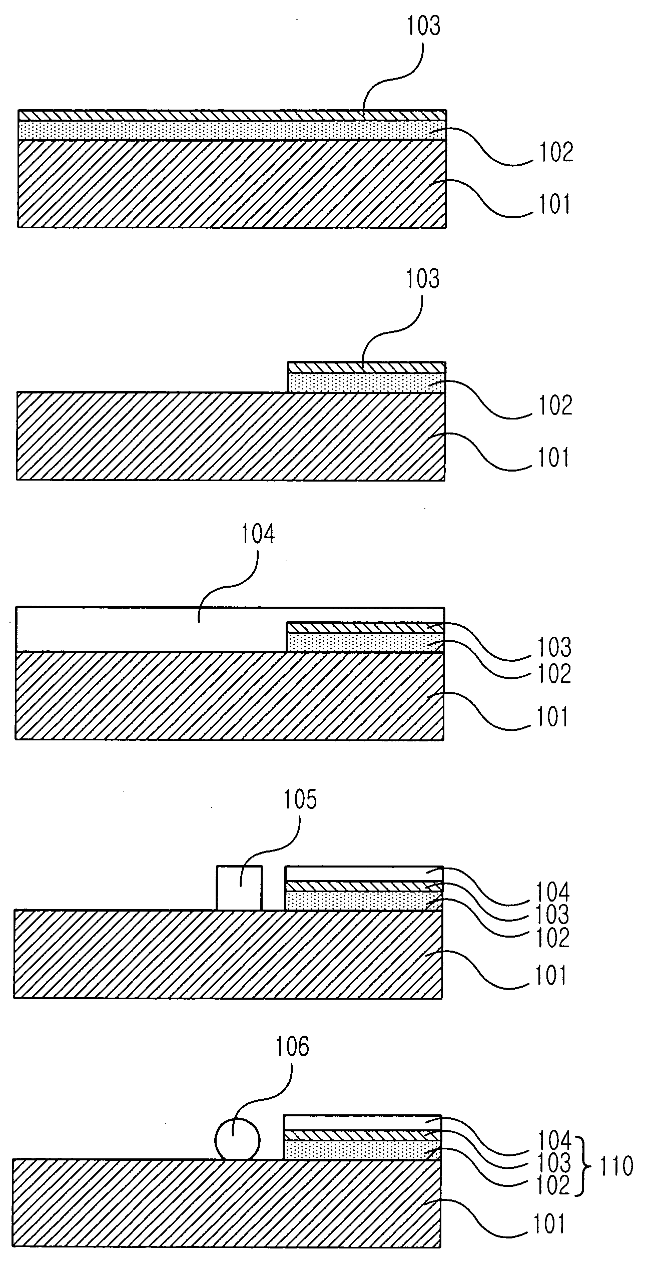
[0036] A preferred embodiment of the present invention will be described herein below with reference to the accompanying drawings. In the following description, well-known functions or constructions are not described in detail since they would obscure the invention in unnecessary detail.

[0037]FIGS. 5A to 5D are views sequentially illustrating a micro-lens fabricating method according to a preferred embodiment of the present invention.

[0038] In FIG. 5A, an SiO2 thin film 52, which is doped with GeO2, P2O5, B2O3, etc., is formed on a silicon or quartz substrate 51 by Flame Hydrolysis Deposition (FHD) orChemical Vapor Deposition (CVD).

[0039] In FIG. 5B, the photoresist (PR) patterns 53 are formed on the thin film 52 by photolithography. The shape of the PR patterns 53 can be polygonal or circular, depending on the shape, diameter, and height of an intended lens.

[0040] In FIG. 5C, thin-film structures 54 are formed in a three-dimensional shape such as a cylinder or a polygonal colum...


PUM

PropertyMeasurementUnit
heightaaaaaaaaaa
distanceaaaaaaaaaa
thicknessaaaaaaaaaa

Abstract

A method of fabricating a micro-lens, and a method of fabricating an optical module using the method are provided. To fabricate a micro-lens, a thin film is formed of a material for the micro-lens on a substrate. A photoresist pattern is formed on the thin film, a thin-film structure is formed by etching the thin film using the photoresist pattern, and the micro-lens is completed by reflow by thermally treating the thin-film structure.

Description

CLAIM OF PRIORITY [0001] This application claims priority under 35 U.S.C. § 119 from an application entitled “Method of Fabricating Micro-lens and Method of Fabricating Optical Module Using the Method,” filed in the Korean Intellectual Property Office on Jul. 1, 2003 and assigned Ser. No. 2003-44410, the contents of which are incorporated herein by reference. BACKGROUND OF THE INVENTION [0002] 1. Field of the Invention [0003] The present invention relates generally to a micro-lens. More particularly, the present invention relates to a method of fabricating a micro-lens and a method of fabricating an optical module having a micro-lens integrated therein using the method. [0004] 2. Description of the Related Art [0005] Micro-lenses are becoming increasingly popular today and can be found components such as optical sensors, optoelectronic products, and optical communications such as optical coupling between optical devices including an optical fiber, a PLC (Planar Lightwave Circuit), a...

Claims


Application Information

Patent Timeline
Patent Type & Authority Applications(United States)
IPC IPC(8): G02B1/10G02B6/42G02B3/00G03F7/00G03F7/20
CPCG02B3/0018G03F7/0005G02B6/4204G02B3/0056G02B3/00
Inventor CHO, JAE-GEOLJUNG, SUN-TAE
Owner SAMSUNG ELECTRONICS CO LTD
Why Eureka
Try Eureka