Method for oxidation of silicon substrate

a technology of silicon substrate and oxidation method, which is applied in the direction of semiconductor/solid-state device manufacturing, basic electric elements, electric devices, etc., can solve the problems of limited ultrathin oxide regime, difficult control of method, and difficult control of method scale, etc., and achieve high precision

Inactive Publication Date: 2004-07-08
NANOS APS
View PDF3 Cites 12 Cited by
  • Summary
  • Abstract
  • Description
  • Claims
  • Application Information

AI Technical Summary

Benefits of technology

0014] It is the purpose of this invention to provide a method for the controlled and scaleable oxidation of silicon where the...

Problems solved by technology

Thermal oxidation, including rapid thermal oxidation, by oxygen exposure at temperatures above 700.degree. C. is the most well known method to achieve thick oxide layers, but has it limitations for the ultrathin oxide regime.
34 (1994), the method is very difficult to control, as it is a balance between surface etching and oxide growth.
Achieving ultrathin layers, that is to say from one layer up to 50 layers, in a controlled way demands a very thorough control of the actual process parameters such as dosing and heating phase, temperature ramping and cooling speed, making this method very hard to control and to scale.
As the oxidation happens continuously at the higher temperatures, the method is not suited for the controlled growth of laye...

Method used


Image

  • Method for oxidation of silicon substrate
  • Method for oxidation of silicon substrate
  • Method for oxidation of silicon substrate

Examples


Embodiment Construction

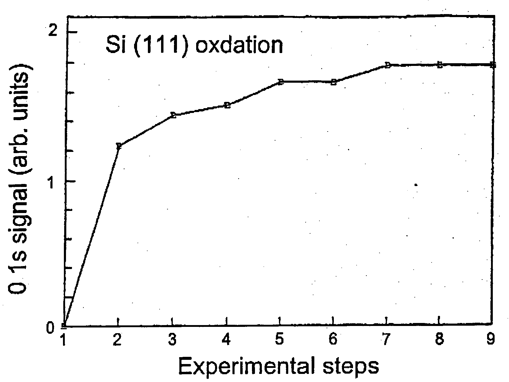
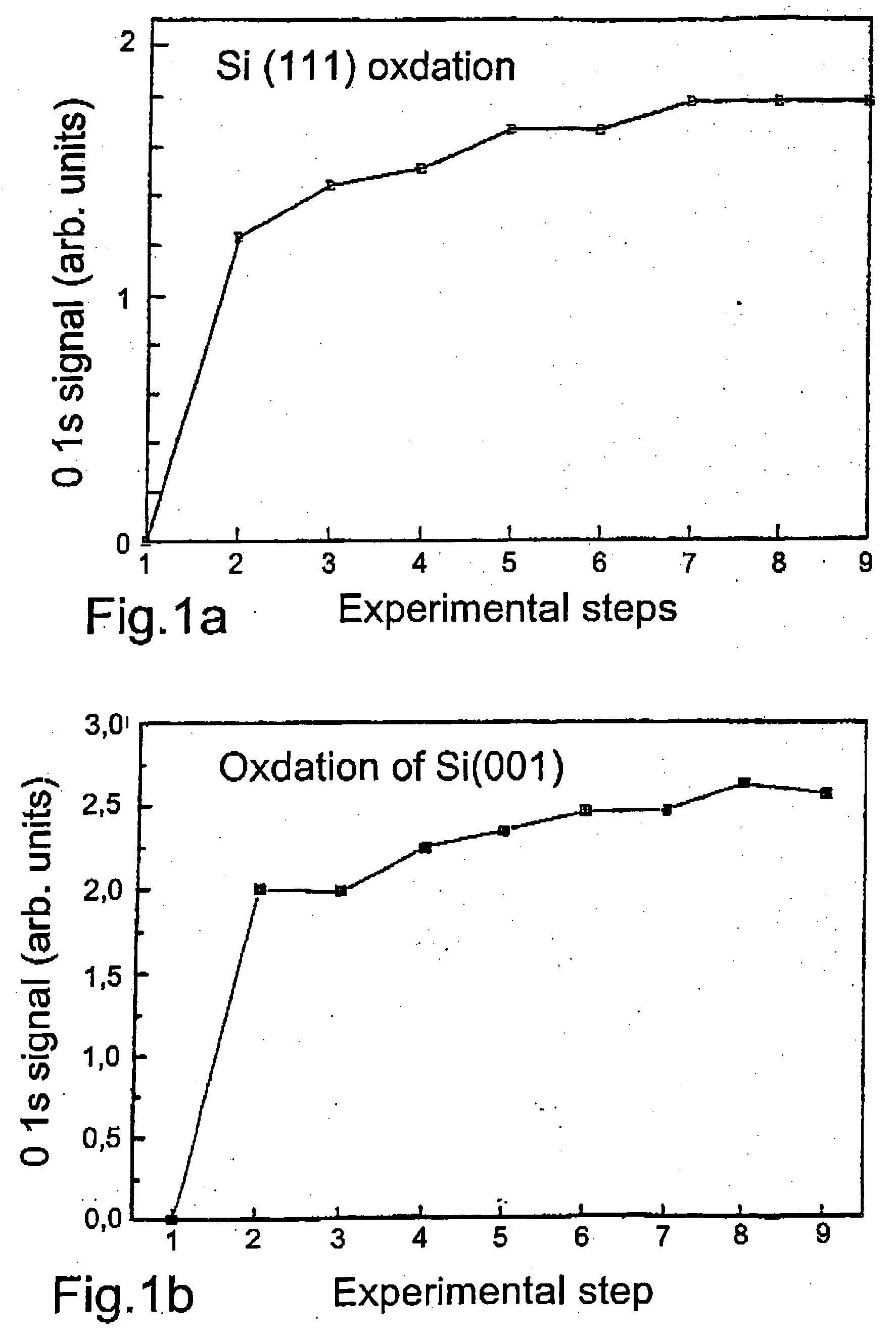
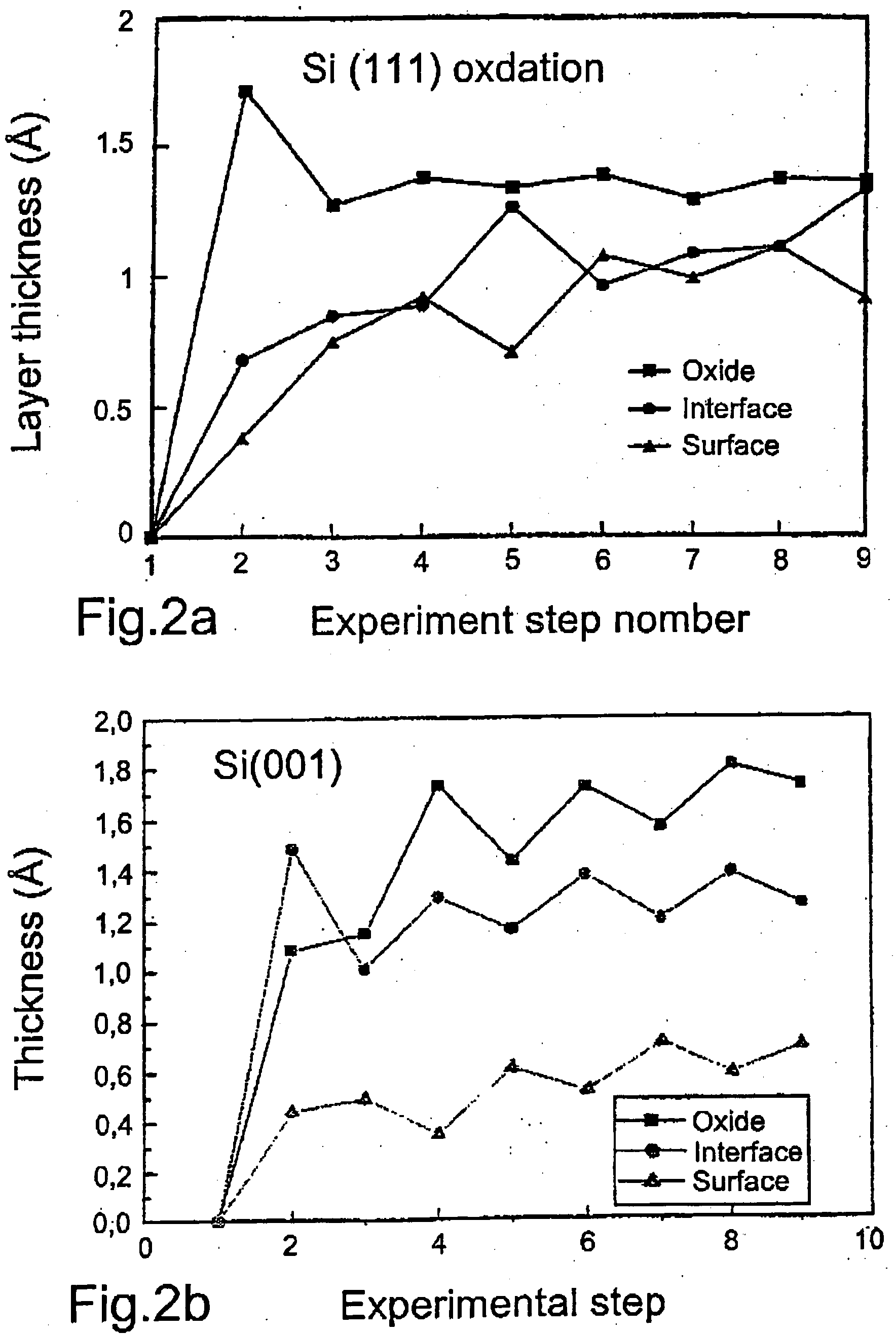
[0037] In the following, a number of experiments will be described, which have been performed in order to demonstrate the growth of oxide layers on silicon in a controlled way with a specified thickness.

[0038] For preparation of the substrate, a standard procedure was used as a cleaning process of polished single crystal silicon wafers, which in the experiments were of n-type with a resistivity of 5 ohm-cm and oriented in (111) or (001) directions. However, crystals with other resistivities and orientations can be used as well.

[0039] The substrates were flash heated to 1000.degree. C. a number of times, after which the surfaces were clean and reconstructed in the known structures as could be monitored with LEED (Low Energy Electron Diffraction), Photoemission, and Optical Second Harmonic Generation Spectroscopy.

Creation of One Monolayer of Oxide (or Oxide-like Substance) (First Recipe)

[0040] In order to produce a silicon oxide layer on the silicon substrate, where the oxide layer ha...


PUM


Abstract

Method for oxidation of a silicon substrate under ultrahigh vacuum base conditions, wherein the substrate undergoes a number of oxidation cycles with exposure to oxygen and heat treatment for converting the adsorbed oxygen into silicon oxide.

Description

[0001] The present invention relates to a method for oxidising silicon under ultrahigh vacuum base conditions.[0002] The semiconductor industry is continuously aiming at increasing the switching speed of transistors in order to increase the performance of computers. One of the most critical aspects for increased speed is the reduction of the width of the MOS (Metal-Oxide-Semiconductor) transistor gate and--correspondingly, following certain recognised scaling rules--the reduction of the thickness of the gate oxide. This oxide is the insulating layer between the semiconductor surface inversion layer through which current flows in parallel with the surface and the gate electrode of the transistor, which turns on and off the inversion condition, and thus the current flow. Typically, insulating silicon dioxide layers on silicon in transistors of year 2000 are between 20 and 100 molecular layers thick, and there is an assumed limit of thickness to withstand electron tunnelling of about 1...

Claims


Application Information

Patent Timeline
IPC IPC(8): H01L21/316
CPCH01L21/02238H01L21/31662H01L21/02299H01L21/02255
Inventor MORGEN, PERPEDERSEN, KJELDT.AE BUTTED.KER, LARS-BOJENSEN, THOMASDAM, FLEMMING KHOFFMANN, SOREN V
Owner NANOS APS
Why Eureka
Try Eureka