
Eureka
For R&D, Eureka makes reading and utilizing patents & technical documents easy.
Eureka AIR
Designed for self-driven R&D workflows. Generate viable solutions, solve complex R&D challenges, empower your innovation with AI.

Eureka Materials
Designed for material experts only. Revolutionize your material R&D, from search, analyze, to developing new materials.

TechResearch
Generate reliable direction feasibility study reports for your R&D in just a few steps.

TechSeek
Discover and master advanced knowledge NOW. Basics, ideas, possibilities, all at once.

TechMind
As an expert in R&D Theories, TechMind can generates customized viable solutions instantly.

TechRisk
Analyze your overall solution with one click, know your potential R&D risks in advance.

TechMonitor
Get weekly tech updates, stay abreast of the latest tech innovations and key insights.
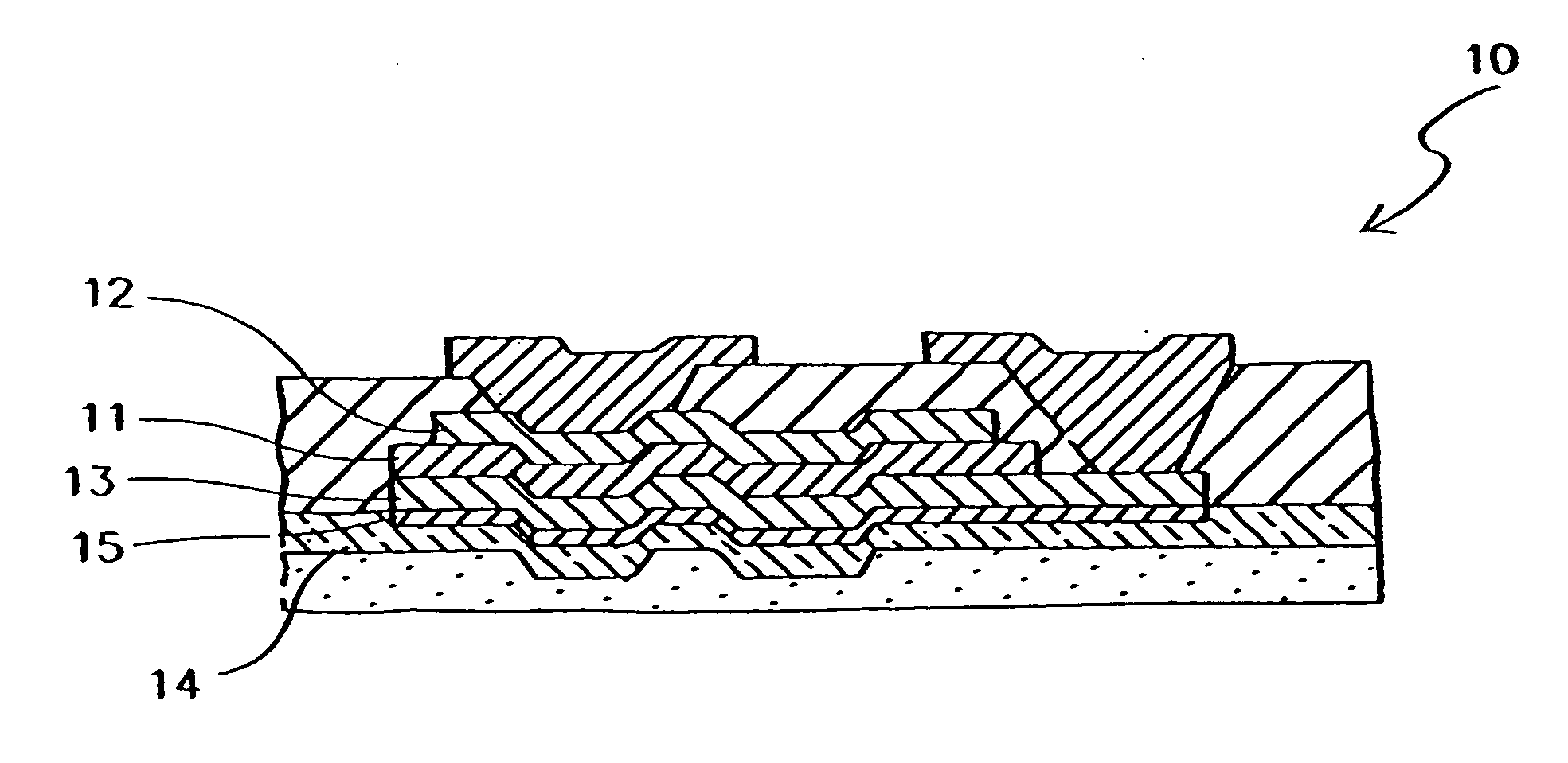
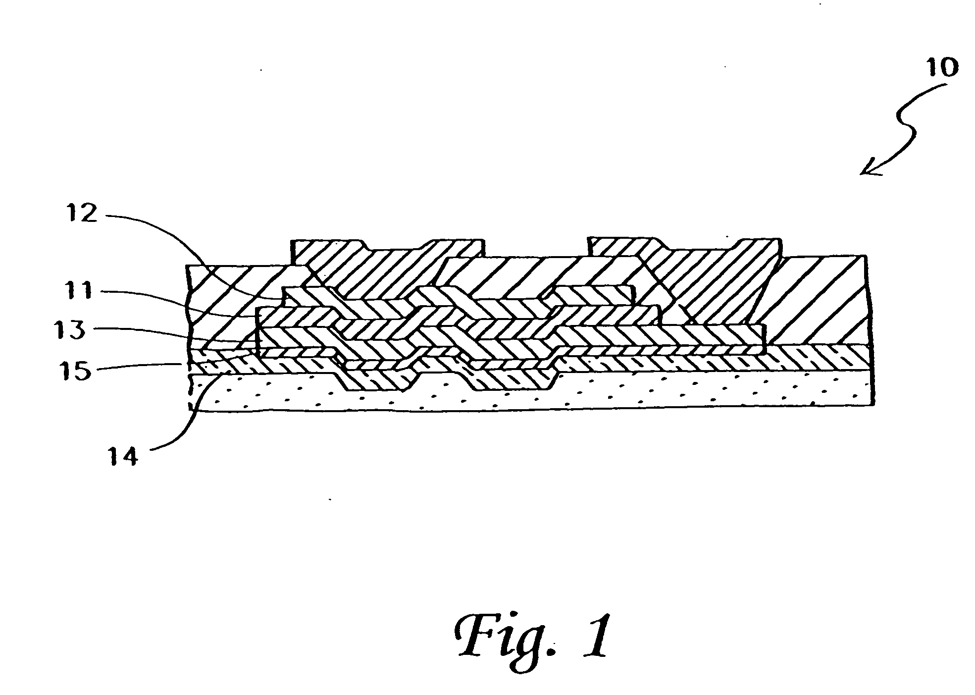
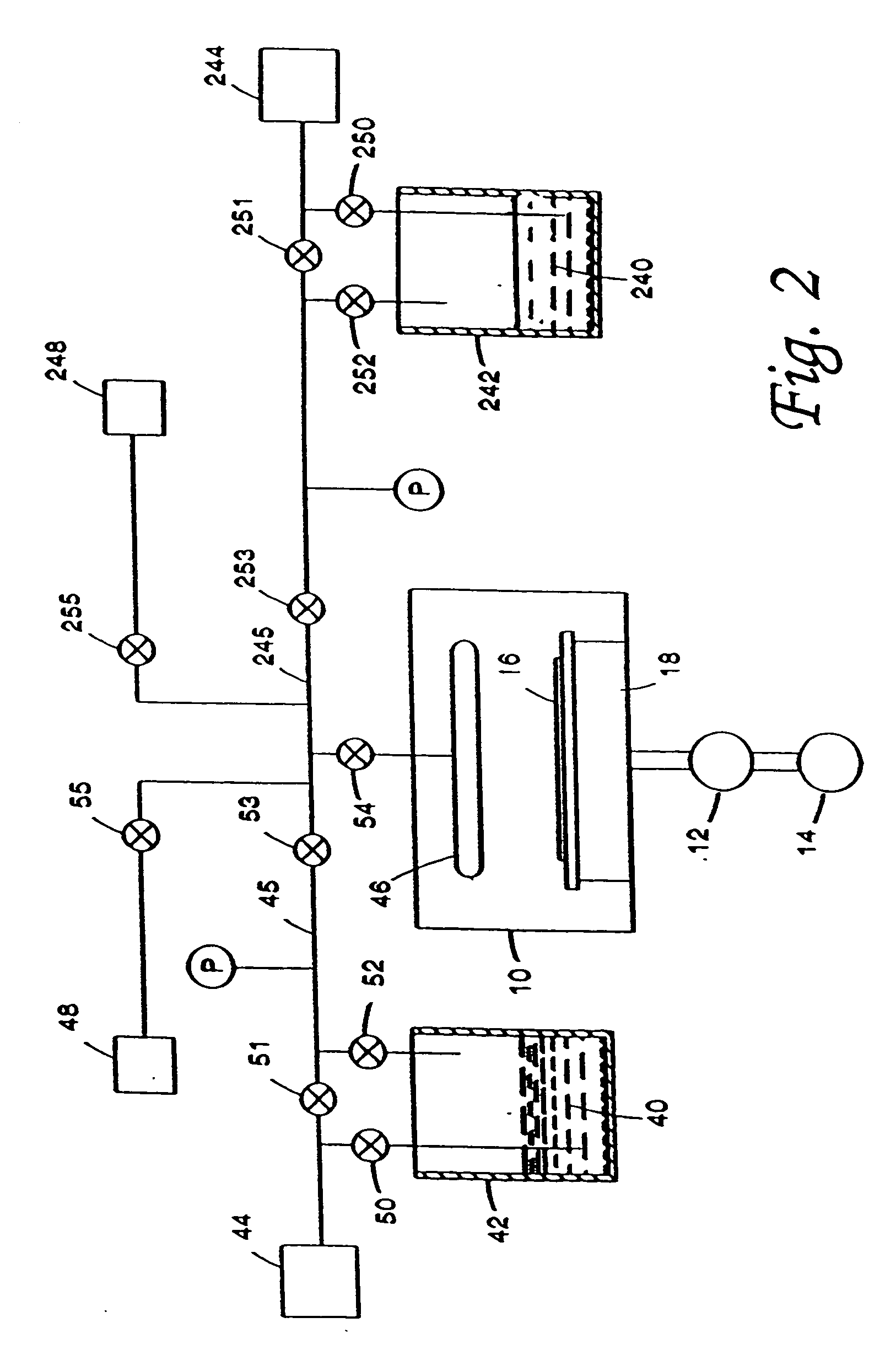
Devices containing platinum-iridium films and methods of preparing such films and devices
- Summary
- Abstract
- Description
- Claims
- Application Information
AI Technical Summary
Benefits of technology
Problems solved by technology
Method used
Image

Examples
examples
The following examples are offered to further illustrate the various specific and preferred embodiments and techniques. It should be understood, however, that many variations and modifications may be made while remaining within the scope of the present invention.
Synthesis of {(CH3)C5H4}Ir(CO)2
In an inert-atmosphere glove box, a flask was charged with 2.0 g (6.4 mmol) of chlorotricarbonyliridium (I) (Strem Chemicals, Inc., Newburyport, Mass.). The compound was suspended in 100 mL of hexanes and stirred during the addition of a solution of methylcyclopentadienyl lithium (12.8 mL of 0.5 M in THF). The flask was equipped with a condenser and the mixture was refluxed for 24 hours. The solvent was then removed in vacuo. The crude product was purified by vacuum distillation; an orange colored liquid product collected was at 58° C. at approximately 200 mTorr. The product was characterized by IR and NMR spectroscopy.
CVD of a Platinum-Iridium Film
A substrate of silicon that had been th...
PUM
| Property | Measurement | Unit |
|---|---|---|
| Electrical conductor | aaaaa | aaaaa |
Abstract
Description
Claims
Application Information
 - R&D Engineer
- R&D Manager
- IP Professional
- Industry Leading Data Capabilities
- Powerful AI technology
- Patent DNA Extraction
Browse by: Latest US Patents, China's latest patents, Technical Efficacy Thesaurus, Application Domain, Technology Topic, Popular Technical Reports.
© 2024 PatSnap. All rights reserved.Legal|Privacy policy|Modern Slavery Act Transparency Statement|Sitemap|About US| Contact US: help@patsnap.com