Undoped oxide liner/BPSG for improved data retention

a data retention and oxide liner technology, applied in the direction of semiconductor devices, electrical devices, transistors, etc., can solve the problems of data retention loss, undesirable delays in production, and difficulty in filling gaps, so as to improve reliability, improve data retention, and improve data retention

Active Publication Date: 2005-01-13
INFINEON TECH LLC
View PDF4 Cites 7 Cited by
  • Summary
  • Abstract
  • Description
  • Claims
  • Application Information

AI Technical Summary

Benefits of technology

[0005] An advantage of the present invention is a method of manufacturing flash memory semiconductor devices with improved data retention and improved reliability.
[0006] Another advantage of the present invention is a flash memory semiconductor device having improved data retention and improved reliability.
[0007] Additional advantages and other features of the present invention will be set forth in the description which follows and in part will be apparent to those having ordinary skill in the art upon examination of the following or may be learned from the practice of the present invention. The advantages of the present invention may be realized and obtained and particularly pointed out in the appended claims.
[0008] According to the present invention, the foregoing and other advantages are achieved in part by a method of manufacturing a semiconductor device, the method comprising: forming two gate electrode structures, spaced apart by a gap, on a semiconductor substrate; depositing an undoped oxide liner on the gate electrode structures and into the gap; and depositing a layer of boron (B) and phosphorous (P)-doped silicon oxide (BPSG) on the undoped oxide liner filling the gap.
[0009] Embodiments of the present invention inc

Problems solved by technology

Various issues arise in attempting to satisfy the ever increasing demands for miniaturization, particularly in fabricating non-volatile semiconductor devices, such as flash memory devices, e.g., electrically erasable programmable read only memory (EEPROM) devices.
As miniaturization proceeds apace, various

Method used


Image

  • Undoped oxide liner/BPSG for improved data retention
  • Undoped oxide liner/BPSG for improved data retention

Examples


Embodiment Construction

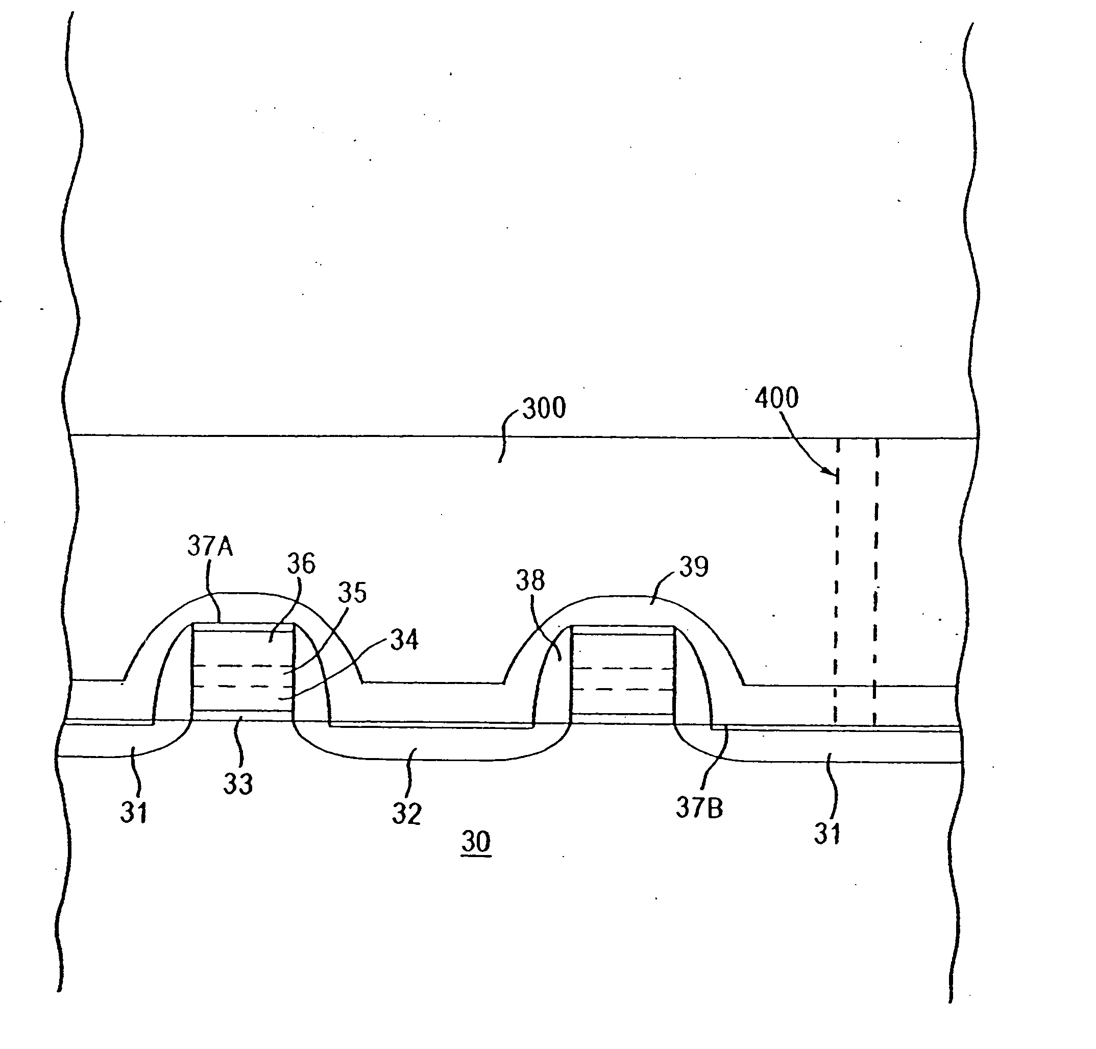
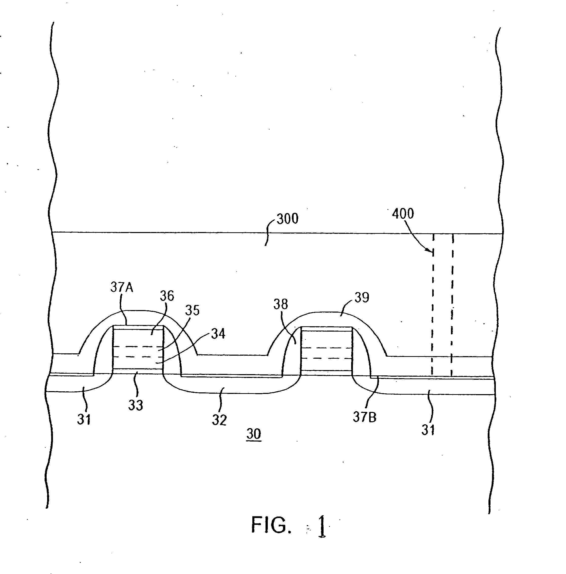
[0013] The present invention addresses and solves various reliability problems which arise in fabricating microminiaturized semiconductor devices, such as flash memory devices, e.g., data retention and gap filling. The present invention provides efficient methodology enabling the fabrication of semiconductor devices exhibiting greater reliability and improved data retention.

[0014] Upon conducting experimentation and investigation, it was postulated that mobile hydrogen ions in the conventional silicon nitride etch stop layer overlying the gate electrode structure degrade the ONO stack causing data retention issues. The present invention addressees and solves such data retention problems by strategically removing the conventional silicon nitride liner and replacing it with an undoped oxide liner prior to depositing the first interlayer dielectric (ILD0).

[0015] It was found that the strategic use of an undoped silicon oxide liner in lieu of the conventional silicon nitride liner con...


PUM


Abstract

Semiconductor devices with improved data retention are formed by depositing an undoped oxide liner on spaced apart transistors followed by in situ deposition of a BPSG layer. Embodiments include depositing an undoped silicon oxide liner derived from TEOS, as at a thickness of 400 Å to 600 Å, on transistors of a non-volatile semiconductor device, as by sub-atmospheric chemical vapor deposition, followed by depositing the BPSG layer in the same deposition chamber.

Description

FIELD OF THE INVENTION [0001] The present invention relates to a method of manufacturing semiconductor devices having high reliability and improved data retention. The present invention has particular applicability in manufacturing high density, multi-level flash memory devices with improved data retention and improved gap filling. BACKGROUND ART [0002] Various issues arise in attempting to satisfy the ever increasing demands for miniaturization, particularly in fabricating non-volatile semiconductor devices, such as flash memory devices, e.g., electrically erasable programmable read only memory (EEPROM) devices. The demands for continuing miniaturization have led to the fabrication of flash memory devices comprising transistors having a gate width of about 0.13 micron and under and gate structures spaced apart by a small gap of about 0.30 micron or less. In accordance with conventional practices, an oxide sidewall spacer is formed on side surfaces of the gate stack, thereby reducin...

Claims


Application Information

Patent Timeline
IPC IPC(8): H01L21/316H01L21/8247H01L27/115H01L29/51
CPCH01L21/02129H01L21/02164H01L21/022H01L21/02271H01L29/511H01L21/31625H01L27/115H01L27/11521H01L21/31612H10B69/00H10B41/30
Inventor NGO, MINH VANHUI, ANGELACHENG, NINGPARK, JEYONGYANG, JEAN YEE-MEIHUERTAS, ROBERT A.KAMAL, TAZRIENGAO, PEI-YUANGOTTIPATI, TYAGAMOHAN
Owner INFINEON TECH LLC
Why Eureka
Try Eureka