Method of manufacturing laminated structure, laminated structure, display device and display unit

a technology of laminated structure and display device, which is applied in the direction of discharge tube luminescnet screen, instrument, and semiconductor/solid-state device details, etc., can solve the problems of large loss of light reflected by the first electrode to be extracted, defect of organic light-emitting device, etc., to prevent side etching, reduce defects, and improve the effect of shap

Inactive Publication Date: 2005-01-13
SONY CORP
View PDF14 Cites 66 Cited by
  • Summary
  • Abstract
  • Description
  • Claims
  • Application Information

AI Technical Summary

Benefits of technology

[0014] In an embodiment, the present invention provides a method of manufacturing a laminated structure capable of preventing side etching resulting from a difference in etching rate on etching a plurality of layers so as to have a favorable shape after etching, a laminated structure, a display device and a display unit which are manufactured through the method.
[0015] Further, the present invention in an embodiment provides a method of manufacturing a laminated structure capable of reducing defects and obtaining high reliability by using a remover which has no corrosivity to silver and a silver alloy of the plurality of layers and an excellent removing property, and is capable of removing impurities causing a dark point defect on removing a mask (photoresist film) after etching the plurality of layers at once, a laminated structure, a display device and a display unit which are manufactured through the method.

Problems solved by technology

Conventionally, the first electrode is made of chromium or the like, so there is a problem that the light absorbance of the first electrode is large, thereby a loss of light reflected by the first electrode to be extracted is large.
However, in a wet etching technique conventionally used for patterning silver, when a laminated structure including the buffer thin film layer disposed on the surface of the silver layer is used as the first electrode, a difference in etching rate between the silver layer and the buffer thin film layer results in side etching of the silver layer, thereby a defect in the shape of the first electrode may cause a defect in the organic light-emitting device.
However, in the case where 2-aminoethanol is used, the photoresist on the buffer thin film layer cannot be removed completely, so it is considered that remained impurities may cause defects such as a dark point defect.
Further, when the photoresist remained after etching silver or the silver alloy is removed with a photoresist remover including 2-aminoethanol, silver or the silver alloy exposed to a side surface of the first electrode may be corroded by the remover, thereby resulting in a defect.

Method used


Image

  • Method of manufacturing laminated structure, laminated structure, display device and display unit
  • Method of manufacturing laminated structure, laminated structure, display device and display unit
  • Method of manufacturing laminated structure, laminated structure, display device and display unit

Examples


first embodiment

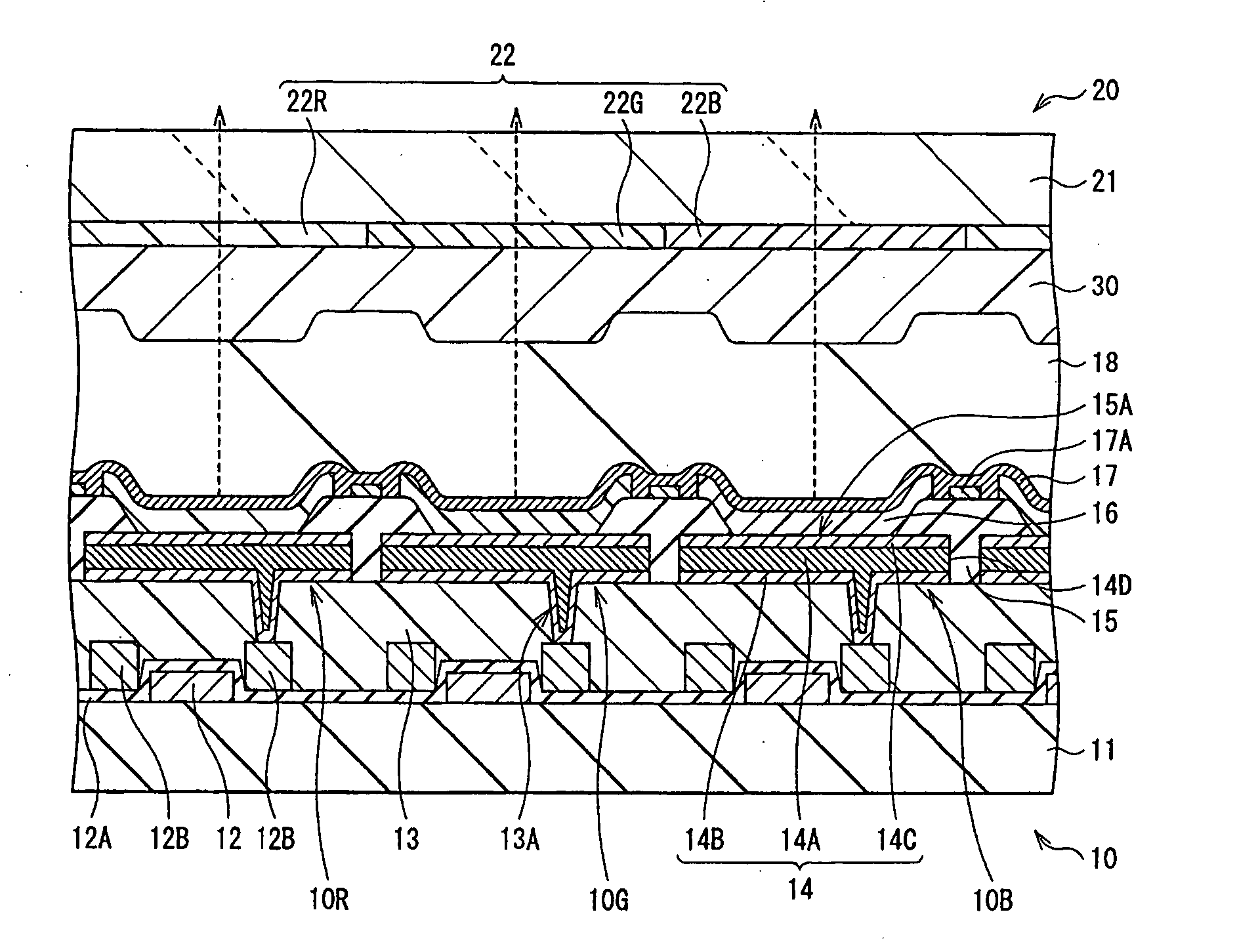
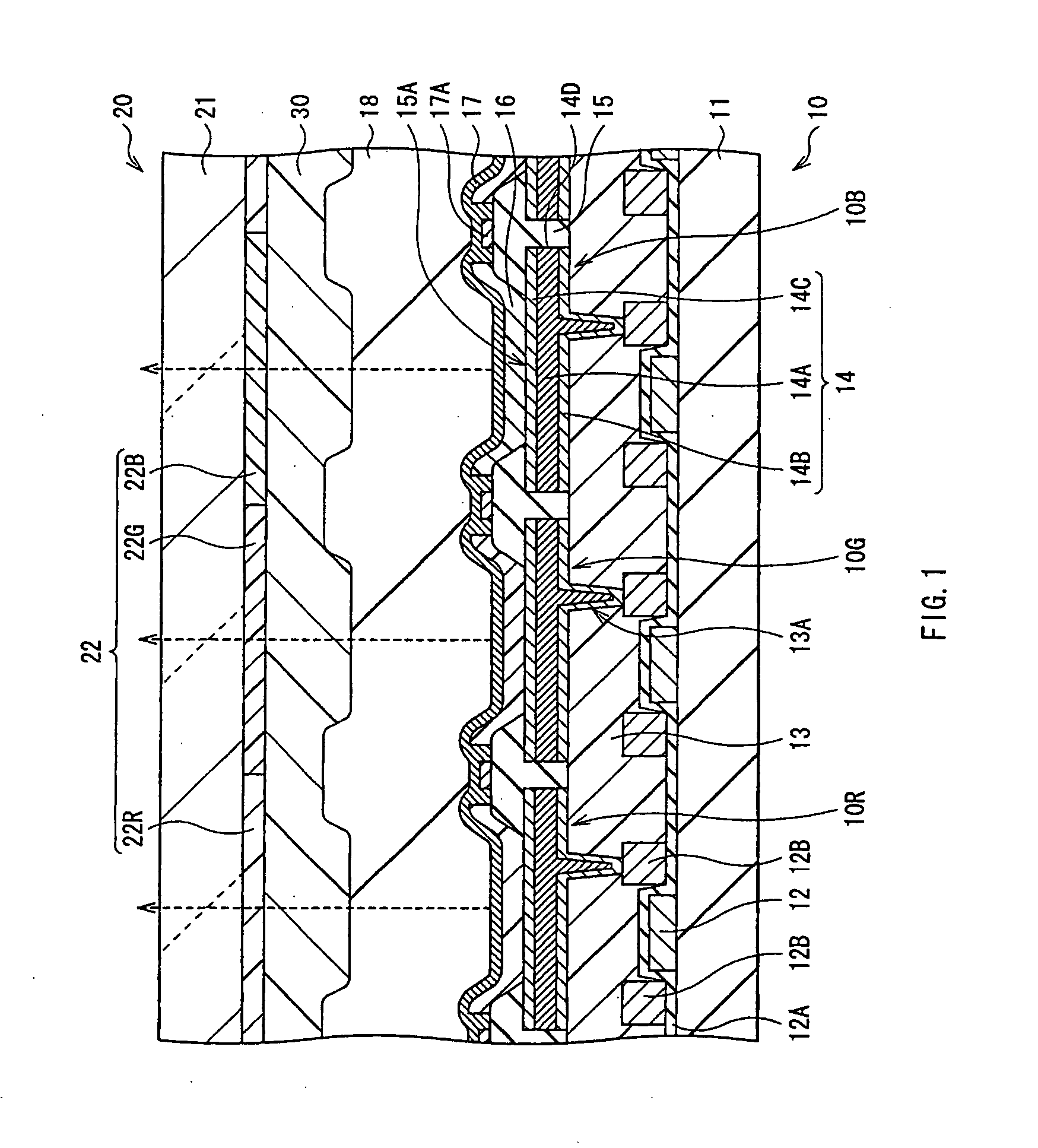
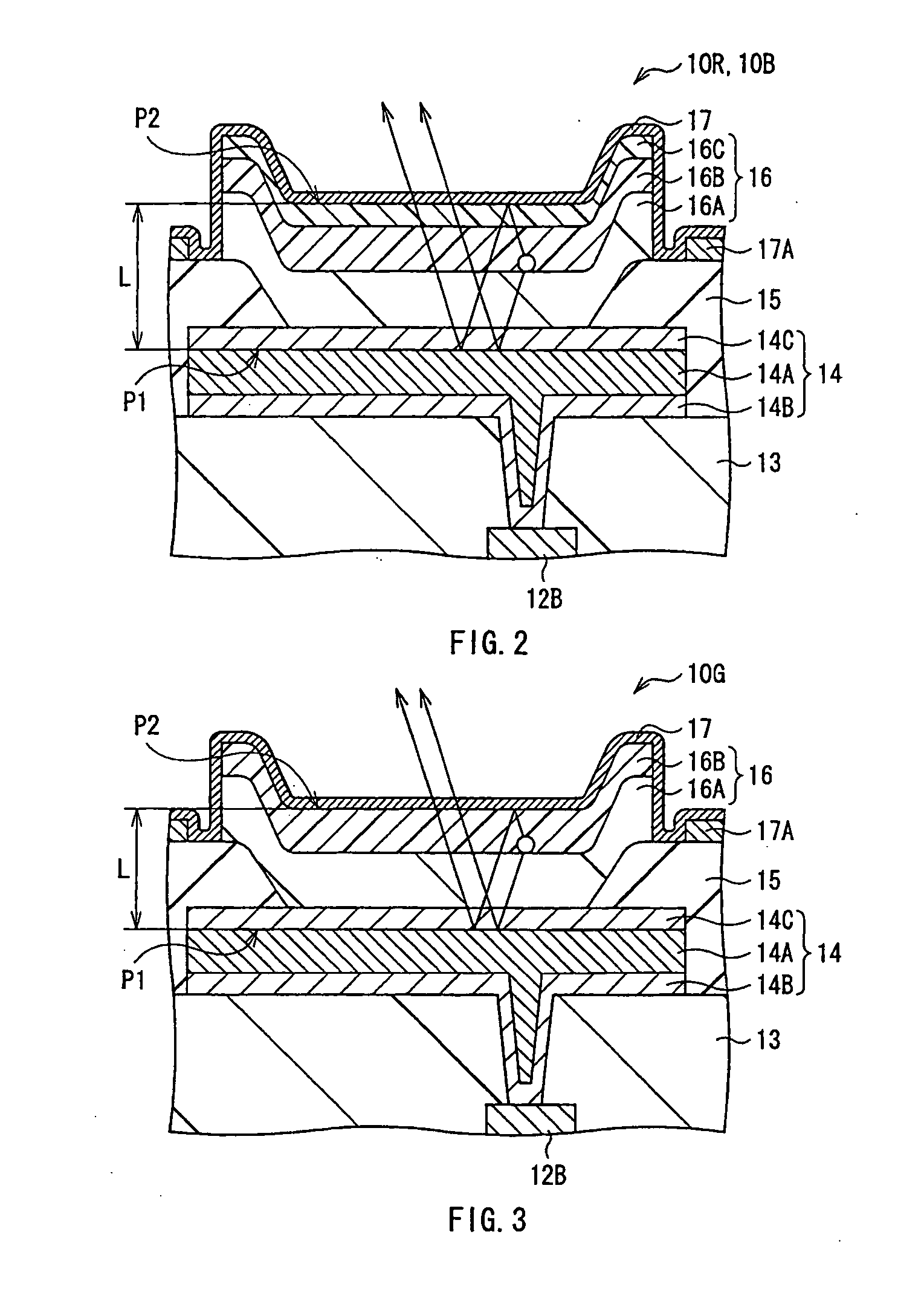
[0042]FIG. 1 shows a sectional view of a display unit according to the invention. The display unit is used as an ultra-thin organic light-emitting display, and in the display unit, a driving panel 10 and a sealing panel 20 face each other, and the whole facing surfaces thereof are bonded together with an adhesive layer 30 made of a thermosetting resin. The driving panel 10 includes, for example, an organic light-emitting device 1OR emitting red light, an organic light-emitting device 10G emitting green light and an organic light-emitting device 10B emitting blue light disposed in order in a matrix shape as a whole on a substrate 11 made of an insulating material such as glass with a TFT 12 and a planarizing layer 13 in between.

[0043] A gate electrode (not shown) of the TFT 12 is connected to a scanning circuit (not shown), and a source and a drain (both not shown) are connected to wiring 12B through an interlayer insulating film 12A made of, for example, silicon oxide, PSG (phosphos...

second embodiment

[0108]FIG. 15 shows a sectional view of a display unit according to the invention. The display unit is used as a transmissive-reflective (semi-transmissive) liquid crystal display, and a drive panel 60 and an opposing panel 70 face each other, and a liquid crystal layer 80 is disposed between them.

[0109] In the drive panel 60, a pixel electrode 62 is formed in a matrix shape on a substrate 61 made of, for example, glass. On the substrate 61, an active driving circuit including a TFT 63 as a drive device electrically connected to the pixel electrode 62, wiring 63A and the like is formed. An alignment film 64 is disposed all over a surface of the substrate 61. On the other hand, a polarizing plate 65 is disposed on the other surface of the substrate 61. Moreover, the laminated structure 14 equivalent to that according to the first embodiment is disposed between the surface of the substrate 61, and the TFT 63 and the wiring 63A. An insulating film 66 is disposed between the laminated s...


PUM

PropertyMeasurementUnit
thicknessaaaaaaaaaa
thicknessaaaaaaaaaa
thicknessaaaaaaaaaa

Abstract

A method of manufacturing a laminated structure capable of being patterned into a favorable shape by preventing side etching is provided. After an adhesive layer made of ITO or the like, a reflective layer made of silver or an alloy including silver, and a barrier layer made of ITO or the like are laminated in order on a substrate with a planarizing layer which is a base layer in between, a mask is formed on the barrier layer, and the adhesive layer, the reflective layer and the barrier layer are etched at once by using the mask to form a laminated structure. As an etching gas, for example, a gas including methane (CH4) is preferable. The laminated structure is used as an anode, and an insulating film, an organic layer including a light-emitting layer and a common electrode as a cathode are laminated in order on the laminated structure so as to form an organic light-emitting device. The laminated structure can be used as a reflective electrode, a reflective film or wiring of a liquid crystal display.

Description

CROSS REFERENCES TO RELATED APPLICATIONS [0001] This application claims priority to Japanese Patent Application Nos. P2003-153052 filed on May 29, 2003, and P2003-305285 filed on Aug. 28, 2003, the disclosures of which are incorporated by reference herein. BACKGROUND OF THE INVENTION [0002] The present invention generally relates to a laminated structure, a display device and a display unit that employ same and methods of manufacturing same. More specifically, the present invention relates to a method of manufacturing a laminated structure which is suitable as a reflective electrode, a reflective film or wiring, and a laminated structure, a display device and a display unit which are manufactured through the method. [0003] In recent years, as one of flat panel displays, an organic light-emitting display using an organic light-emitting device has become a focus of attention. The organic light-emitting display is of a self-luminous type, so it is considered that the organic light-emit...

Claims


Application Information

Patent Timeline
Patent Type & Authority Applications(United States)
IPC IPC(8): G02F1/1335G02F1/1343H05B33/26H01L21/28H01L21/3205H01L21/3213H01L21/77H01L21/84H01L23/52H01L27/32H01L51/50H01L51/52H01L51/56H05B33/10
CPCG02F1/133553G02F1/13439H01L27/1214H01L27/3211H01L27/322H01L27/3244H01L2251/5315H01L51/5228H01L51/5234H01L51/5237H01L51/5265H01L51/56H01L51/5218H10K59/35H10K59/38H10K59/12H10K50/818H10K50/824H10K50/828H10K50/8423H10K50/852H10K50/8426H10K2102/3026H10K50/844H10K71/00H05B33/10
Inventor YOKOYAMA, SEIICHIOHWADA, TAKUOISHIKAWA, NORIO
Owner SONY CORP
Why Eureka
Try Eureka