Power semiconductor module with detector for detecting main circuit current through power semiconductor element

a technology of semiconductor elements and detectors, applied in thermoelectric instruments, dc-ac conversion without reversal, instruments, etc., can solve the problems of increased module cost, high cost and power loss associated with shunt resistance, etc., and achieve the effect of reducing the size of the wiring area, and reducing the cost of the modul

Active Publication Date: 2005-01-13
MITSUBISHI ELECTRIC CORP
View PDF8 Cites 9 Cited by
  • Summary
  • Abstract
  • Description
  • Claims
  • Application Information

AI Technical Summary

Benefits of technology

[0013] In accordance with the first aspect of the invention, main circuit current is detected by means of a bonding wire instead of a shunt resistance. As a result, power loss in the detector is lower, the size of a wiring area can be smaller and the circuit can be simplified, allowing the cost of the module to be reduced.
[0014] Preferably, either one of the first and second circuit patterns has a region adjacent to and generally parallel to the bonding wire so that the region and the bonding wire carry current in generally opposite directions. This reduces inductance of the boding wire and therefore wiring inductance of the module.

Problems solved by technology

However, cost and power loss associated with the shunt resistance are high.
Further, since the circuit becomes complicated, the cost of the module is increased.

Method used


Image

  • Power semiconductor module with detector for detecting main circuit current through power semiconductor element
  • Power semiconductor module with detector for detecting main circuit current through power semiconductor element
  • Power semiconductor module with detector for detecting main circuit current through power semiconductor element

Examples


first embodiment

[0026] First Embodiment

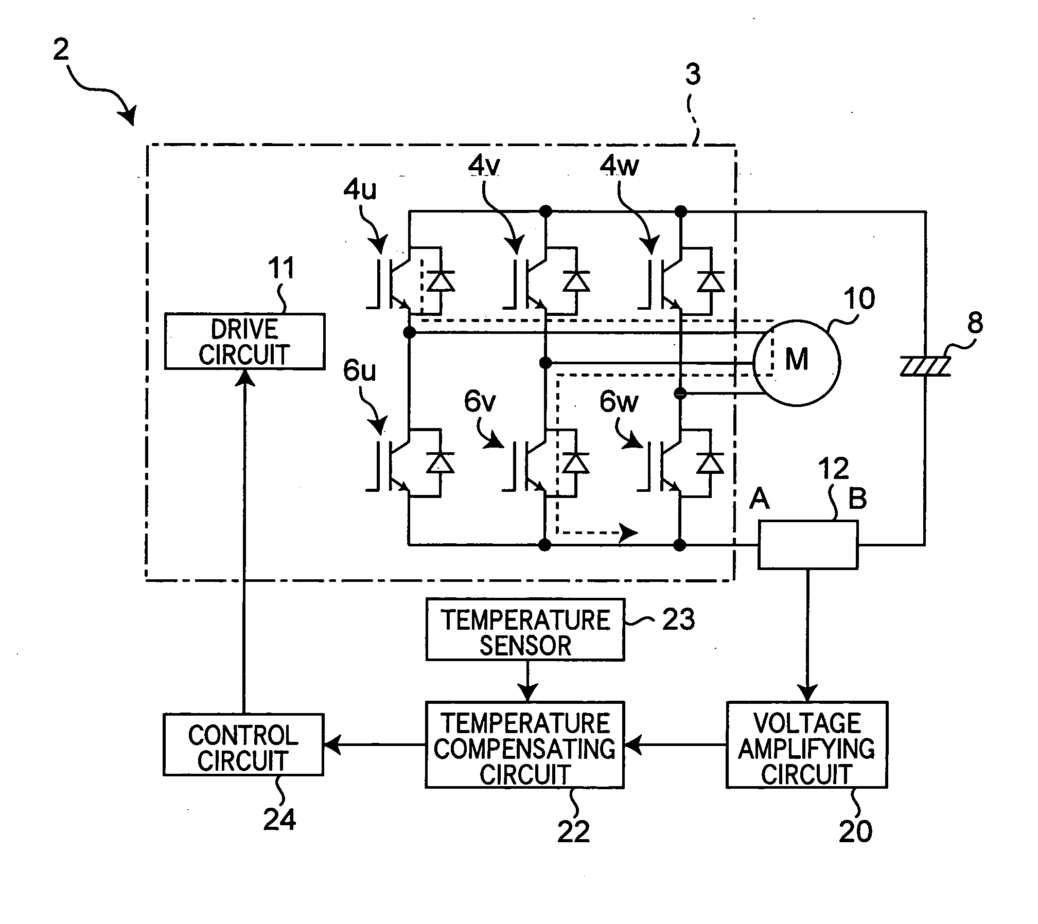
[0027] Referring to FIG. 1, there is shown a power semiconductor module, which is a first embodiment according to the present invention. The module 2 includes switching elements or IGBTs 4u, 4v, 4w, 6u, 6v and 6w connected in parallel and series with each other, which constitute an inverter circuit 3. Specifically, the switching elements 4u, 4v and 4w are U-phase, V-phase and W-phase elements of the upper arm, respectively, and their collector terminals are connected with the cathode of a DC power supply or electrolytic capacitor 8. The switching elements 6u, 6v and 6w are U-phase, V-phase and W-phase elements of the lower arm, respectively, and their emitter terminals are connected with the anode of the DC power supply 8. The emitter terminal of the U-phase switching element 4u of the upper arm is connected with the collector terminal of the U-phase switching element 6u of the lower arm and with an external load or motor 10. The emitter terminal of the V-phas...

second embodiment

[0040] Second Embodiment

[0041] Referring to FIG. 3, a second embodiment of the present invention will be described hereinafter. In a description below, components identical or similar to those in the first embodiment are indicated by identical reference numbers or those with suffixes. The power semiconductor module 2a of the embodiment has a function to protect the switching elements where overcurrent is flown due to, for example, an excessive load to the motor 10 or short circuit. (i.e. current passes through the pair of switching elements connected in: parallel with each other). Specifically, the drive circuit 11a of the inverter circuit 3a for actuating the switching elements 4u, 4v, 4w, 6u, 6v and 6w is connected with a pair of voltage detection terminals not shown, which is connected with the terminal patterns 18 and 19 (FIG. 2) of the detector 12, so that the drive circuit receives a signal indicative of a potential difference across the bonding wire 16 (FIG. 2). For instance,...

third embodiment

[0044] Third Embodiment

[0045] Referring to FIG. 4, a third embodiment of the present invention will now be described. Each of the power semiconductor modules of the present embodiment and embodiments described later is similar to the module 2 shown in FIG. 1 except that circuit patterns of the detector for detecting a potential difference across the bonding wire are different from those in the first embodiment.

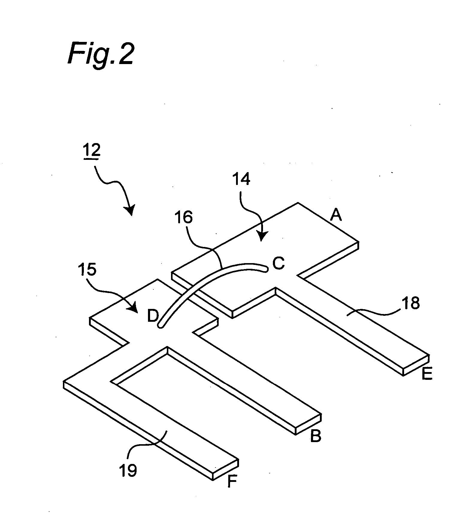
[0046] In the embodiment, like the detector 12 of the power semiconductor module 2, the detector 12b includes a pair of circuit patterns 14b and 15b connected via the bonding wire 16. A pair of terminal patterns 18b and 19b is extended from near bonding points C and D of the pair of the circuit patterns 14b and 15b, respectively. The pair of terminal patterns 18b and 19b is connected at output ports E and F with a pair of voltage detection terminals not shown with high impedance. In the embodiment, the circuit pattern 15b is formed so that a portion thereof (region G) is adja...


PUM


Abstract

A power semiconductor module has a detector for detecting main circuit current passing through a power semiconductor element. The detector includes first and second circuit patterns; a bonding wire connected at first and second bonding points with the first and second circuit patterns, respectively; and a pair of terminal patterns extended from near the first and second bonding points of the first and second circuit patterns. The detector is designed to detect a potential difference between the pair of terminal patterns generated by flowing main circuit current through the first circuit pattern, the bonding wire and then the second circuit pattern, in order to detect a potential difference across the bonding wire.

Description

RELATED APPLICATION [0001] This application is based on Japanese Patent Application No. 2003-273300, the content of which being incorporated herein by reference. BACKGROUND OF THE INVENTION [0002] 1. Field of the Invention [0003] The present invention relates to a power semiconductor module, and in particular to a power semiconductor module having a detector for detecting main circuit current passing through a power semiconductor element. The present invention also relates to a system for determining the main circuit current. [0004] 2. Description of the Related Art [0005] Conventionally, there has been known a power semiconductor module in which main circuit current passing through a power semiconductor element is detected in order to prevent a breakdown of the element due to overcurrent or to feedback control an external load, as disclosed in, for example, Japanese Patent Publication No. 6-112614. [0006] In general, in order to detect main circuit current through a power semicondu...

Claims


Application Information

Patent Timeline
Patent Type & Authority Applications(United States)
IPC IPC(8): H01L21/822H01L27/04H01L23/34H01L23/62H02M1/00H02M7/48H05K1/02
CPCH01L23/34H01L2924/1301H01L2924/3011H02M7/003H02M2001/0009H01L2224/48091H01L23/62H01L2924/13055H01L2924/13091H01L2924/19107H01L2924/30107H01L2924/1305H01L2924/00014H01L2924/00H02M1/0009H05K1/02
Inventor IWAGAMI, TORUSHIRAKAWA, SHINYASEO, MAMORUSAKAI, MASAKIWANG, DONG
Owner MITSUBISHI ELECTRIC CORP
Why Eureka
Try Eureka