Liquid crystal display element and method of producing the same

a liquid crystal display and liquid crystal technology, applied in the direction of liquid crystal compositions, instruments, chemistry apparatus and processes, etc., can solve the problems of cholesteric liquid crystals that are difficult to maintain the focal conic state, the distinctive feature of cholesteric liquid crystals, and the loss of bistability, etc., to achieve the effect of high quality

Inactive Publication Date: 2005-01-13
MINOLTA CO LTD
View PDF11 Cites 16 Cited by
  • Summary
  • Abstract
  • Description
  • Claims
  • Application Information

AI Technical Summary

Benefits of technology

A primary object of the invention is to provide a liquid crystal display element capable of image display with high quality.
Another object of the invention is to provide a liquid crystal display element capable of image display with high contrast.
Still another object of the invention is to provide a liquid crystal display element capable of image display with good color purity.
In the liquid crystal light (optical) modulation element including a pair of substrates and a liquid crystal layer held between the substrates and including a liquid crystal material, which exhibits a cholesteric phase in a room temperature and has a peak of a selective reflection wavelength in a visible wavelength range, a mixed state of a polydomain state and a monodomain state may be attained in the liquid crystal domains of the pixel regions near at least one of the substrates holding the liquid crystal layer in the selective reflection state. Alternatively, the polydomain state may be achieved in each of the liquid crystal domains of the pixel regions near the substrates of the liquid crystal layer in the selective reflection state. Thereby, the liquid crystal in the liquid crystal domains in the pixel region near one of the opposite substrates may have the cholesteric helical axes different in angle with respect to a normal of the substrate from that of the other substrate. Thereby, the reflected light can be collected on the front surface on the element observation side, and the good image display with high brightness, contrast and color purity can be performed. Further, when no external stimulus (e.g., no voltage) is applied, the display state (image display with high brightness, contrast and color purity) can be maintained for a long term.

Problems solved by technology

If the above liquid crystal element is used as the display element, therefore, the viewability becomes extremely low.
The rubbing of the thin polyimide film increases the restricting force on a polyimide interface so that it becomes difficult to maintain the focal conic state.
Consequently, the bistability, which is the distinctive feature of the cholesteric liquid crystal, may be lost.
According to this method, however, mixing of the polymer in the liquid crystal material may lower the reliability of the element, and / or may require the increased drive voltage.
In this method, however, domains including different directions of the inclined helical axes (directions of the helical axes projected onto the substrate) are formed randomly so that scattering of the incident light is liable to occur due to the difference in refractive index between the domains, resulting in lowering of the purity of the display color in the selective reflection.
In a multilayer liquid crystal display element employing a multilayer structure for multicolor display, the reflection light from the lower layer is liable to be affected by light scattering by an upper layer, which lowers both the contrast and color purity.
Therefore, the liquid crystal domains form the monodomain state on the whole substrate so that the stability in the focal conic state is liable to lower, and the bistability, which is the feature of the cholesteric liquid crystal element, is may be impaired.
In the planar orientation state, the inclination of helical axes of the liquid crystal on the random domain side is gradually lost, which impairs the long-term bistability.
In any one of the above case, it is difficult to maintain the display state (good display state with high contrast and color purity) for a long time without voltage application, and it is difficult to achieve the intended characteristics for high contrast and high color purity together with the bistability.
Therefore, the molecules of the liquid crystal in such region cannot be controlled.
This results in the following disadvantage.
In general, as compared with the case of only the planar state alone, the domains are small in the case where the two states are mixed, and therefore incident light is liable to scatter.
Further, selective reflection of the incident light may partially occur.
This deteriorates the display characteristics of the liquid crystal display element.
However, when performing, e.g., the black display by a light absorbing layer Bk in the focal conic state of the liquid crystal in the pixels, the black display is blurred due to the selective reflection and scattering of the incident light by the liquid crystal between the pixels, resulting in low contrast of the image display.
Further, since the selective reflection and scattering of the incident light are caused by the liquid crystal between the pixels, and the liquid crystal between the pixels scatters the light, which is selectively reflected by the lower layer toward the observation side, these lower the color purity in display.
In any one of the above cases, the optimum solution has not yet achieved in connection with the orientation control of the liquid crystal in the above types of liquid crystal display element.

Method used


Image

  • Liquid crystal display element and method of producing the same
  • Liquid crystal display element and method of producing the same
  • Liquid crystal display element and method of producing the same

Examples


example 1

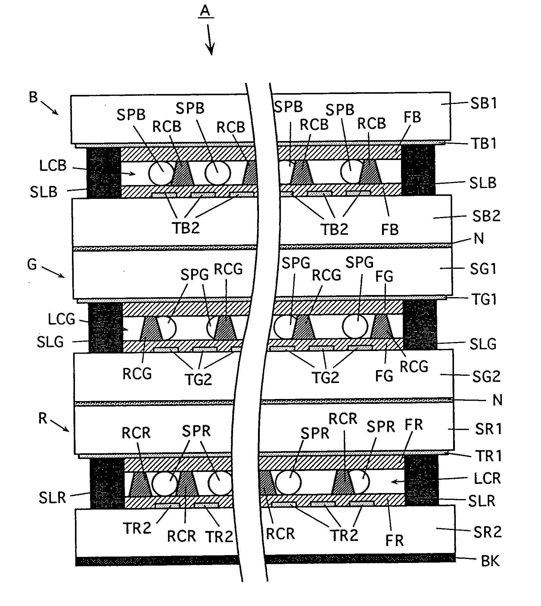
This example is a three-layer liquid crystal display element of the reflection type using glass substrates, in which the rubbing processing is effected on a portion of each orientation film in each liquid crystal display element corresponding to the liquid crystal in the non-pixel region.

The liquid crystal display elements B, G and R were produced in the foregoing methods, and then were successively layered and bonded by the adhesives N.

In each element, 7059 glass substrate (manufactured by Corning Inc.) was used as each substrate. On each substrate, belt-like transparent ITO electrodes were formed in parallel with each other. The belt-like electrodes had a width of 300 μm, and were arranged with a pitch of 340 μm.

On all the surfaces of the substrates in contact with the liquid crystal, there were formed the orientation films made of polyimide AL8044 (manufactured by JSR Corp.). Rubbing processing was effected on a portion of each orientation film corresponding to the non-ima...

example 2

In each liquid crystal display element, the orientation film, which could be subjected to optical orientation processing, was formed on each of the substrate surfaces in contact with the liquid crystal, and the optical orientation processing was effected on the film portion corresponding to the non-pixel region. Structures other than the above were the same as those of the example 1.

The optical orientation was performed in the following manner. First, a photomask of the same configuration as the electrode pattern was arranged on the substrate, which was coated with polyimide, i.e., the orientation film material similar to that of the example 1, and was registered with the electrode pattern on the substrate. The above structure was irradiated with ultraviolet light. A lamp for emitting the ultraviolet light was a mercury lamp having a central wavelength of 365 nm. The emitting direction of the ultraviolet light formed 75° with respect to the normal of the substrate. The irradiatio...

example 3

A plurality of substrates of 0.2 μm in thickness, made of polycarbonate manufactured by Teijin Limited, were employed. Each substrate was provided with transparent belt-like ITO electrodes parallel to each other. Each transparent electrode had a width of 300 μm and was arranged with a pitch of 330 μm.

All the surfaces of each substrate in contact with the liquid crystal were provided with polyimide films AL8044 manufactured by JSR Corp., and the rubbing processing was effected in the following manner on the portion of the polyimide film in the non-pixel region.

First, positive resist of about 1 μm in thickness was uniformly applied to the polyimide film by a table coater. A photomask provided with holes of configurations corresponding to the electrode pattern was arranged on the substrate coated with the resist, and the exposure by the exposing device was performed. By the development after the exposure, the resist between the pixels, i.e., the resist in the non-pixel region was ...


PUM

PropertyMeasurementUnit
widthaaaaaaaaaa
widthaaaaaaaaaa
thicknessaaaaaaaaaa

Abstract

(1) A liquid crystal display element including a liquid crystal layer including liquid crystal contained between a pair of substrates and exhibiting a cholesteric phase, wherein an orientation film is arranged on at least one of the paired substrates, and is in contact with the liquid crystal layer, and liquid crystal molecular orientation processing for portions of each orientation film corresponding to pixel regions are effected in a manner different from that effected on at least a portion of a portion corresponding to non-pixel region of the orientation film on at least one of the substrates. (2) A liquid crystal light modulation element including a liquid crystal layer held between a pair of substrate and including a liquid crystal material exhibiting a cholesteric phase in a room temperature and having a peak of a selective reflection wavelength in a visible wavelength range, wherein the liquid crystal layer in the selective reflection state has pixel regions neighboring to the opposite substrates, respectively, and liquid crystal domains in the pixel regions neighboring to at least one of the substrates are in a mixed state of a polydomain state and a monodomain state.

Description

CROSS REFERENCE TO RELATED APPLICATION The invention is based on patent application Nos. 2000-199023 Pat., 2000-236810 Pat. 2001-72054 Pat., and 2001-72911 Pat. filed in Japan, the entire contents of which are hereby incorporated by reference. BACKGROUND OF THE INVENTION 1. Field of the Invention The present invention relates to a liquid crystal display element, and in other words, a liquid crystal light modulation element and method of producing the same. 2. Description of the Background Art The liquid crystal display element and, in other words, the liquid crystal light modulation element primarily includes a pair of substrates, between which a liquid crystal layer including liquid crystal material is held. For example, predetermined drive voltage is applied to the liquid crystal layer to control orientation of liquid crystal molecules in the liquid crystal layer so that external light incident on the liquid crystal light modulation element is modulated to perform intended di...

Claims


Application Information

Patent Timeline
Patent Type & Authority Applications(United States)
IPC IPC(8): G02F1/136G02F1/1333G02F1/1337G02F1/1347G02F1/137
CPCG02F1/133707G02F1/133753G02F2001/133757G02F1/13718G02F1/1347G02F1/133757G02F1/136
Inventor OKADA, MASAKAZUHASHIMOTO, KIYOFUMIMIYAI, MITSUYOSHI
Owner MINOLTA CO LTD
Why Eureka
Try Eureka