Process for producing semiconductor article using graded epitaxial growth

a technology of epitaxial growth and semiconductors, applied in semiconductor devices, chemistry apparatus and processes, single crystal growth, etc., can solve the problems of limiting the maximum ge composition to a low value, complicating or destroying the silicon layer may also complicate or undermine the performance of devices built, so as to achieve simplified and improved process, high quality material

Inactive Publication Date: 2005-01-13
MASSACHUSETTS INST OF TECH
View PDF99 Cites 61 Cited by
  • Summary
  • Abstract
  • Description
  • Claims
  • Application Information

AI Technical Summary

Benefits of technology

[0010] According to the invention, there is provided an improved technique for production of wide range of high quality material is provided. In particular, the production of relaxed Si1-xGex-on-insulator (SGOI) substrate or relaxed III-V or II-VI material-on-insulator, such as GaAs-on-insulator, is described. High quality monocrystalline relaxed SiGe layer, relaxed Ge l...

Problems solved by technology

One of the main drawbacks is the quality of the resulting Si1-xGex film and BOX.
In addition, Ge segregation during high temperature anneal also limits the maximum Ge composition to a low value.
The silicon layer in the structure is unnecessary, and may complicate or undermine the performance of devices built on it.
For example, it may form a parasitic back channel on this strained-Si, or may confine unwanted electrons due to the band gap offset between the strained-Si and SiGe layer.
The presence of the silicon layer in the above structure may be for the purpose of facilitating Si-insulator wafer bonding, but is unnecessary for ideal SGOI substrates.
Again, the silicon layer may also complicate or undermine the performance of devices built on it.
Fo...

Method used


Image

  • Process for producing semiconductor article using graded epitaxial growth
  • Process for producing semiconductor article using graded epitaxial growth
  • Process for producing semiconductor article using graded epitaxial growth

Examples


Embodiment Construction

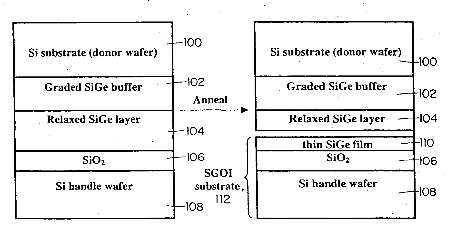
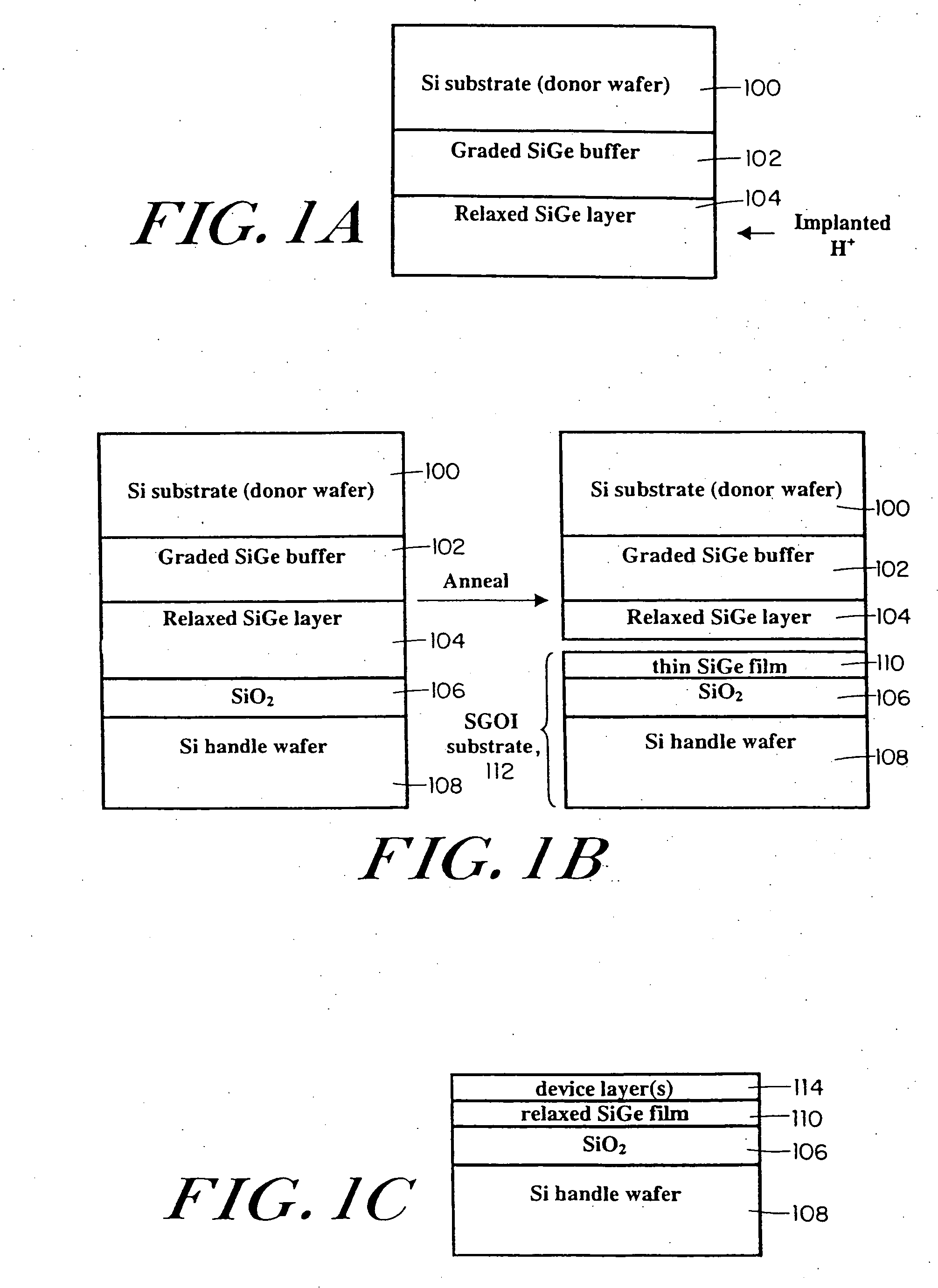
[0019] An example of a process in which SGOI is created by layer transfer is described. The experiment was performed in two stages. In the first stage, heteroepitaxial SiGe layers are formed by a graded epitaxial growth technology. Starting with a 4-inch Si (100) donor wafer 100, a linearly stepwise compositionally graded Si1-xGex buffer 102 is deposited with CVD, by increasing Ge concentration from zero to 25%. Then a 2.5 μm relaxed Si0.75Ge0.25 cap layer 104 is deposited with the final Ge composition, as shown in FIG. 1A.

[0020] The relaxed SiGe cap layer has high quality with very low dislocation defect density (less than 1E6 / cm2), as the graded buffer accommodates the lattice mismatch between Si and relaxed SiGe. A thin layer of this high quality SiGe will be transferred into the final SGOI structure. The surface of the as-grown relaxed SiGe layer shows a high roughness around 11 nm to 15 nm due to the underlying strain fields generated by misfit dislocations at the graded layer...


PUM


Abstract

A process for producing monocrystalline semiconductor layers. In an exemplary embodiment, a graded Si1-xGex (x increases from 0 to y) is deposited on a first silicon substrate, followed by deposition of a relaxed Si1-yGey layer, a thin strained Si1-zGez layer and another relaxed Si1-yGey layer. Hydrogen ions are then introduced into the strained SizGez layer. The relaxed Si1-yGey layer is bonded to a second oxidized substrate. An annealing treatment splits the bonded pair at the strained Si layer, such that the second relaxed Si1-yGey layer remains on the second substrate. In another exemplary embodiment, a graded SixGex is deposited on a first silicon substrate, where the Ge concentration x is increased from 0 to 1. Then a relaxed GaAs layer is deposited on the relaxed Ge buffer. As the lattice constant of GaAs is close to that of Ge, GaAs has high quality with limited dislocation defects. Hydrogen ions are introduced into the relaxed GaAs layer at the selected depth. The relaxed GaAs layer is bonded to a second oxidized substrate. An annealing treatment splits the bonded pair at the hydrogen ion rich layer, such that the upper portion of relaxed GaAs layer remains on the second substrate.

Description

PRIORITY INFORMATION [0001] This application claims priority from provisional application Ser. No. 60 / 225,666 filed Aug. 16, 2000.BACKGROUND OF THE INVENTION [0002] The present invention relates to a production of a general substrate of relaxed Si1-xGex-on-insulator (SGOI) for various electronics or optoelectronics applications, and the production of monocrystalline III-V or II-VI material-on-insulator substrate. [0003] Relaxed Si1-xGex-on-insulator (SGOI) is a very promising technology as it combines the benefits of two advanced technologies: the conventional SOI technology and the disruptive SiGe technology. The SOI configuration offers various advantages associated with the insulating substrate, namely reduced parasitic capacitances, improved isolation, reduced short-channel-effect, etc. High mobility strained-Si, strained-Si1-xGex or strained-Ge MOS devices can be made on SGOI substrates. [0004] Other III-V optoelectronic devices can also be integrated into the SGOI substrate by...

Claims


Application Information

Patent Timeline
IPC IPC(8): H01L21/02H01L21/20H01L21/762H01L27/12H01L21/205
CPCH01L21/02381H01L21/0245H01L21/02502H01L21/0251Y10S438/933H01L21/02532H01L21/02546H01L21/76254H01L21/02521
Inventor CHENG, ZHI-YUANFITZGERALD, EUGENE A.ANTONIADIS, DIMITRI A.HOYT, JUDY L.
Owner MASSACHUSETTS INST OF TECH
Why Eureka
Try Eureka