
Ion sensitive field effect transistor and method for producing an ion sensitive field effect transistor

a technology of field effect transistor and ion sensitive, which is applied in the direction of instruments, electrical equipment, pill delivery, etc., can solve the problems of limited stability of glass electrodes in strong alkali solutions, high production cost of glass electrodes, and inability to use glass electrodes in hydrofluoric acid, etc., to achieve good chemical protection, high operational safety, and good adhesion of substra

Inactive Publication Date: 2005-01-20
FRAUNHOFER GESELLSCHAFT ZUR FOERDERUNG DER ANGEWANDTEN FORSCHUNG EV
View PDF2 Cites 21 Cited by
  • Summary
  • Abstract
  • Description
  • Claims
  • Application Information

AI Technical Summary

Benefits of technology

[0017] It is an advantage of the present invention that by changing the nitrogen content during production, the mechanical and chemical characteristics of the gate material can be adjusted, whereby the ion sensitive field effect transistor can be adjusted with regard to an intended field of application, such as sensitivity.
[0018] It is another advantage of the present invention that the inventive ion sensitive field effect transistor can be operated in a secure way, i.e. without the danger of forming splinters during breakage, whereby it is suitable for fields of application, which require a high operational safety, such as for food technology.
[0019] Further, the inventive ion sensitive field effect transistor can be produced in CMOS compatible planar technology in an inexpensive way, wherein further circuit elements integrated on the chip, which are, for example, used for detecting measurement data, can be generated together with the ion sensitive field effect transistor.
[0020] According to a preferred embodiment of the present invention, an ion sensitive field effect transistor comprises a substrate, on the surface of which a gate of carbon nitride is formed above a channel region by reactive sputtering. Preferably, the gate of carbon nitride has a nitrogen content of 18-30 at % to obtain both a good adhesion of the substrate as well as a good chemical protection.
[0021] In further embodiments, the inventive gate can comprise a layer structure, which has several layers of carbon nitride with different nitrogen content. For forming a good adhesion, the lower layer of the layer structure, which is arranged adjacent to the channel region, has a high nitrogen proportion, and the nitrogen proportion of the layer decreases with increasing distance of the channel region, so that an outer layer has a high chemical resistance due to the low nitrogen proportion.
[0022] In a further embodiment, the inventive gate layer of carbon nitride can comprise a concentration gradient, wherein the concentration of the nitrogen decreases starting from a surface of the layer, which is arranged adjacent to the channel region, with increasing distance of the channel region, so that the outer surface of the layer facing away from the channel region, which comes into contact with a measurement fluid during measuring, has a low nitrogen proportion for achieving a high chemical resistance.

Problems solved by technology

In many aggressive media, glass electrodes can be operated in a stable way, but their stability is restricted in strong alkali solutions.
Further, a usage of glass electrodes in hydrofluoric acid is not possible.
Glass electrodes require a high proportion of manual labor in the production, which is why the same are expensive.
Further, the field of application of glass electrodes is limited since they generate splinters when breaking.
For example, usage of glass electrodes in food technology is not feasible, since the splinters resulting from breakage are dangerous foreign bodies in food.
These are only suitable in a limited way for usage with the above-mentioned requirements, since the gate of Si3N4 is subject to a high drift and has a low longtime stability.
Further, the ion sensitive field effect transistors with a gate of Si3N4 cannot be used in aggressive media over longer periods.
However, ion sensitive field effect transistors with a metal oxide gate have the disadvantage that they do not have sufficient resistance against basic solutions with high temperatures and against hydrofluoric acid.
However, one disadvantage of using amorphous diamond-like carbon, is that layers of this material have a high internal stress, which can reduce the layer adhesion and can lead to peeling off of the layers and consequently to a destruction of the ion sensitive field effect transistor.
Thus, these ion sensitive field effect transistors are not suitable for long-term usage in all fields of application.

Method used


Image

  • Ion sensitive field effect transistor and method for producing an ion sensitive field effect transistor
  • Ion sensitive field effect transistor and method for producing an ion sensitive field effect transistor

Examples


Embodiment Construction

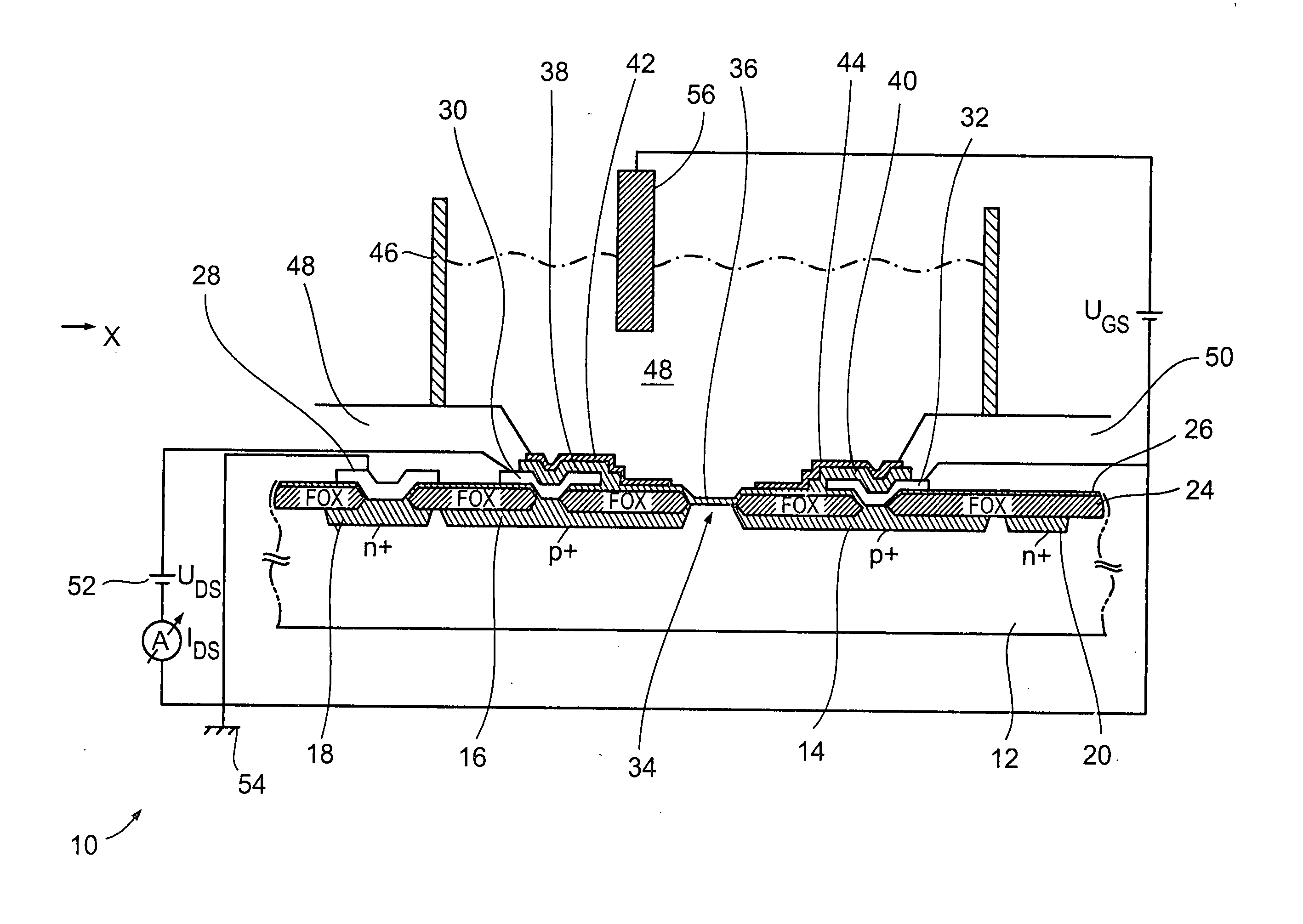
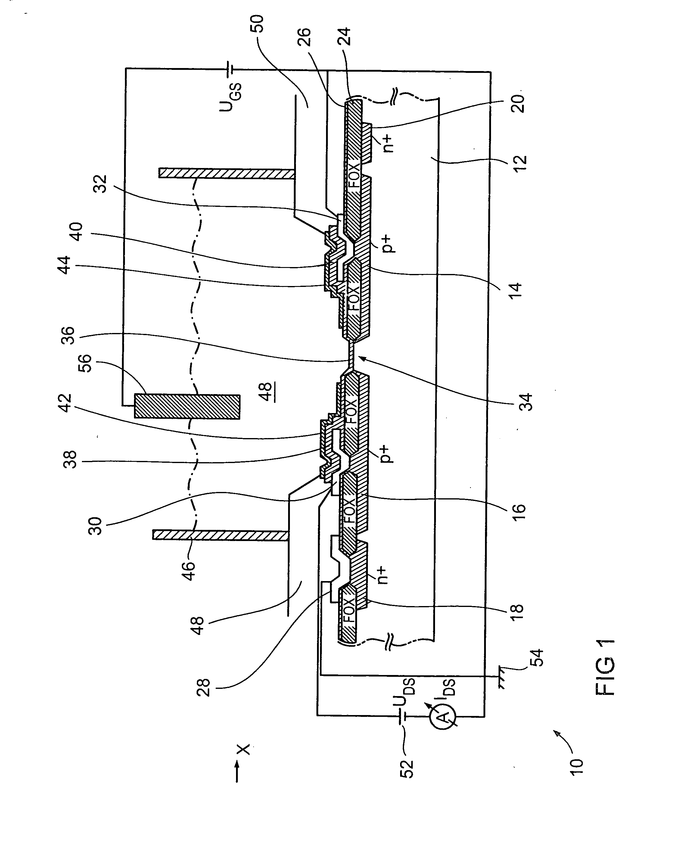
[0025] In FIG. 1, a cross-section representation of an ion sensitive field effect transistor (FET) 10 is shown. The FET 10 comprises a semiconductor substrate 12, such as a silicon substrate. A p+ source region 14 and a p+ drain region 16 are formed in the substrate 12. Further, a first substrate terminal region 18 and a second substrate terminal 20 are formed in the substrate 12, which comprise n+ regions (ohmic contacts). Therefore, the substrate can be a combination of a carrier substrate and an epitaxial layer arranged thereon, wherein the active regions of the device are formed.

[0026] A field oxide layer 24 is formed on a surface of the substrate 12. A further isolating layer 26 is formed on the field oxide layer 24.

[0027] Further, the FET 10 comprises a terminal 28, e.g. of aluminum, which extends through the field oxide layer 24 and the isolating layer 26 and is connected to a first substrate terminal region 18. Further, the FET 10 comprises a drain contact (a drain) 30, wh...


PUM

PropertyMeasurementUnit
Thicknessaaaaaaaaaa
Adhesion strengthaaaaaaaaaa
Adhesivityaaaaaaaaaa

Abstract

The invention relates to an ion-sensitive field effect transistor, comprising a gate (36) consisting of carbon nitride. The carbon nitride gate (36) is highly resistant to aggressive substances to be measured and also exhibits good adhesive properties. In addition, the ion-sensitive field effect transistor has high long-term stability and negligible drift. Said ion-sensitive field effect transistor can be produced in a method that uses CMOS-compatible planar technology.

Description

CROSS-REFERENCE TO RELATED APPLICATION [0001] This application is a continuation of copending International Application No. PCT / EP02 / 01410, filed Feb. 11, 2002, which designated the United States and was not published in English.BACKGROUND OF THE INVENTION [0002] 1. Field of the Invention [0003] The present invention relates to ion sensitive field effect transistors as well as to a method for producing the same. [0004] 2. Description of the Prior Art [0005] Ion sensitive field effect transistors (ISFET) serve as detection elements, for example during measuring a pH value, measuring ions or special substance concentrations. Fields of application for ion sensitive field effect transistors are process measuring technique, analytical chemistry or environmental technology, wherein measurements are typically performed in aqueous solutions or organic mixtures. [0006] Prior to the usage of semiconductor detection apparatuses, glass electrodes were exclusively used for electric transducers f...

Claims


Application Information

Patent Timeline
IPC IPC(8): A61K9/20A61K31/415A61K31/495A61K31/54A61K31/635G01N27/414
CPCG01N27/414
Inventor GRUEGER, HEINRICHKUNATH, CHRISTIAN
Owner FRAUNHOFER GESELLSCHAFT ZUR FOERDERUNG DER ANGEWANDTEN FORSCHUNG EV
Learn More