Surface light emitting semiconductor laser element

a laser element and semiconductor technology, applied in semiconductor lasers, optical elements, instruments, etc., can solve the problems of significant reduction of yield, difficult to produce surface light-emitting, limited tolerance of production errors, etc., and achieve high efficiency

Active Publication Date: 2005-01-20
SONY CORP
View PDF17 Cites 58 Cited by
  • Summary
  • Abstract
  • Description
  • Claims
  • Application Information

AI Technical Summary

Benefits of technology

[0088] When the surface light emitting semiconductor laser element according to one aspect of the present is used in an optical wiring field where the combined optical system is hardly used in view of the costs, it is possible to provide a direct connection with high efficiency. Thus, the surface light emitting semiconductor laser element according to one aspect of the present can be used efficiently.

Problems solved by technology

However, if the size of the current confinement structure is 4 μm or less, the following problems occur.
Firstly, the tolerance of production errors becomes limited, since the size of the current confinement structure is extremely small.
It is difficult to produce a surface light-emitting semiconductor laser element having a current confinement structure with a small diameter with good controllability.
Also, wafer in-plane uniformity becomes poor, resulting in significantly decreased yields.
In other words, since the output depends on the single-peak transverse mode, it is difficult to provide high output from the surface light emitting semiconductor laser element in the single-peak transverse mode.
Thirdly, due to the increased resistance caused by the current confinement, the impedance is mismatched.
Accordingly, it is difficult to apply the surface light emitting semiconductor laser element to light transmission driven at high frequency, as required in the communication field.
However, since light is injected through a substrate, it is difficult to apply this invention to a surface light emitting semiconductor laser element.
In addition, since a proton-injection-type is presumed, it is difficult to apply this invention to the oxidized-type current confinement structure.
However, the process is complicated because a compound semiconductor layer should be re-grown.
There are both technical and economical problems.
As described above, using the conventional technique, it is difficult to provide a surface light emitting semiconductor laser element that emits laser light in the single-peak transverse mode.

Method used


Image

  • Surface light emitting semiconductor laser element
  • Surface light emitting semiconductor laser element
  • Surface light emitting semiconductor laser element

Examples


embodiment 1

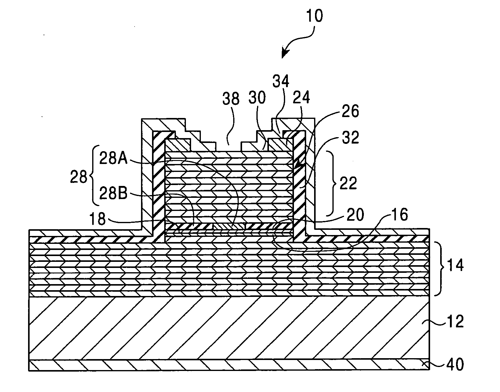
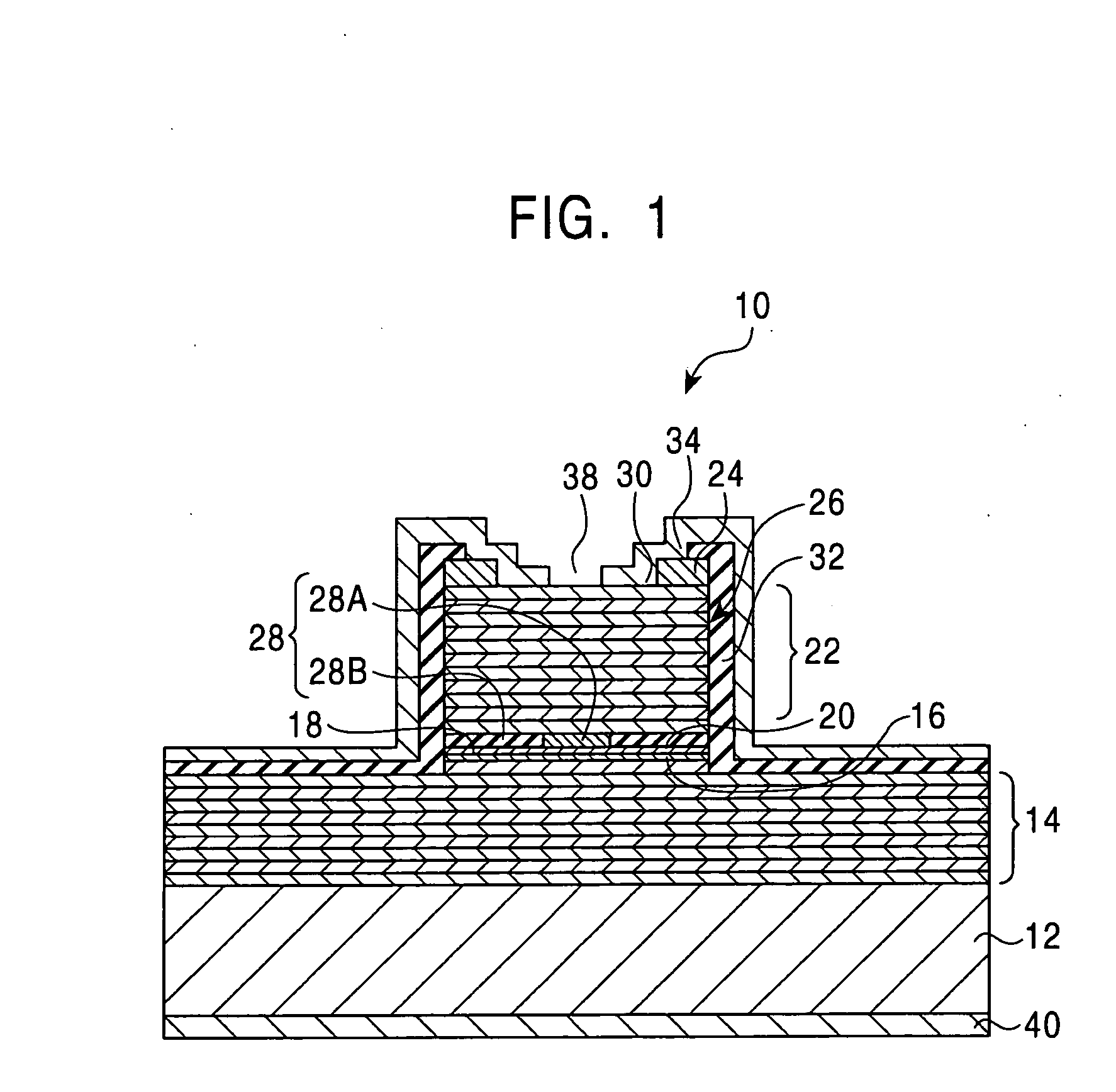
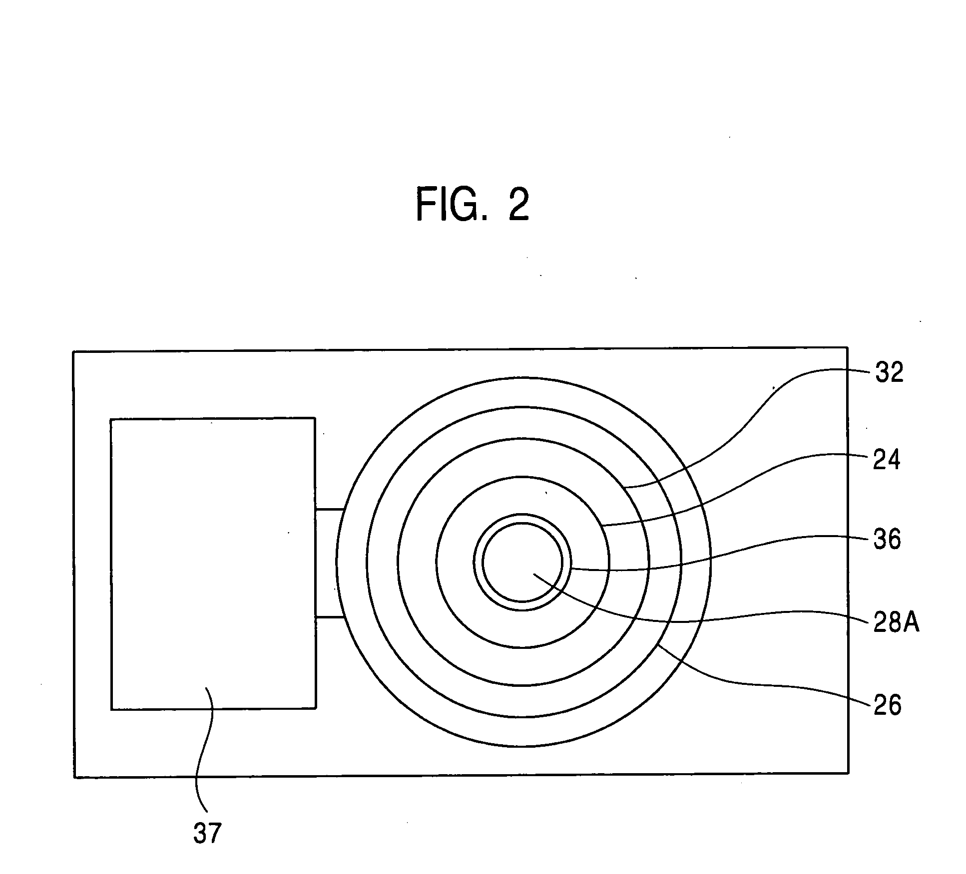
[0115]FIG. 1 shows a sectional view of a surface light emitting semiconductor laser element according to the present invention. FIG. 2 is a top view of the surface light emitting semiconductor laser element. FIG. 3A is a schematic sectional view showing a main part of the surface light emitting semiconductor laser element. FIG. 3B is a schematic sectional view for illustrating functions of the main part corresponding to FIG. 3A.

[0116] As shown in FIG. 1, a surface light emitting semiconductor laser element 10 comprises a laminated structure sequentially comprising an n-type GaAs substrate 12, a lower diffractive bragg reflector (hereinafter “lower DBR”) 14 comprising an n-type semiconductor multi-layer, an Al0.3Ga0.7As lower clad layer 16, a GaAs light emitting layer (active layer) 18, an Al0.3Ga0.7As upper clad layer 20, an upper diffractive bragg reflector 22 (hereinafter “upper DBR”) comprising a p-type GaAs cap layer, and a p-type GaAs contact layer 24 with a film thickness of ...

embodiment 2

[0139]FIGS. 5A, 5B, 6C, 6D, 7E and 7F are sectional views showing steps of manufacturing the surface light emitting semiconductor laser element according to the present invention.

[0140] As shown in FIG. 5A, a lower DBR 14, a lower clad layer 16, a light emitting layer (active layer) 18, an upper clad layer 20, an upper DBR 22, and a p-type GaAs contact layer 24 are sequentially laminated on an n-type GaAs substrate 12 using a MOCVD method or the like.

[0141] Before the upper DBR 22 is formed, an AlAs layer 28 having a film thickness of 30 nm is formed instead of the p-type Al0.9Ga0.1As layer on the layer of the upper DBR 22 at the nearest side of the active layer 18.

[0142] As shown in FIG. 5B, the contact layer 24, the upper DBR 22, the upper clad layer 20, the active layer 18, the lower clad layer 16, and the lower DBR 14 are etched by a dry etching method using a chlorine-based gas to form a cylindrical mesa post 26 having a mesa diameter of 40 μm.

[0143] The laminated structure...

embodiment 3

[0150]FIG. 8 shows a sectional view of an alternative surface light emitting semiconductor laser element according to the present invention.

[0151] The alternative surface light emitting semiconductor laser element has a similar structure in a main part 50 to the surface light emitting semiconductor laser element 10 except that a contact layer 52 and a p-side electrode 54 have different structures.

[0152] As shown in FIG. 8, the contact layer 52 includes three layer: an upper contact layer 52A, a middle contact layer 52B, and a lower contact layer 52C. The impurity concentrations of respective contact layers gradually decrease step-wise from the upper contact layer to the lower contact layer.

[0153] The lower contact layer 52C has, for example, an impurity concentration of 5×10¹⁸, which is the lowest among the three contact layers, and has an opening 56C which is the largest opening. The middle contact layer 52B has, for example, an impurity concentration of 1×10¹⁹, which is higher ...


PUM


Abstract

A surface light emitting semiconductor laser element, comprises a substrate, a lower reflector including a semiconductor multi-layer disposed on the substrate, an active layer disposed on the lower reflector, an upper reflector including a semiconductor multi-layer disposed on the active layer, a compound semiconductor layer having a first opening for exposing the upper reflector and extending over the upper reflector, and a metal film having a second opening for exposing the upper reflector disposed inside of the first opening and extending over the compound semiconductor layer, wherein the metal film and the compound semiconductor layer constitute a complex refractive index distribution structure where a complex refractive index is changed from the center of the second opening towards the outside. A method of emitting laser light in a single-peak transverse mode is also provided.

Description

BACKGROUND OF THE INVENTION [0001] 1. Field of the Invention [0002] The present invention relates to a surface light emitting semiconductor laser element and a method of manufacture thereof. More particularly, the present invention relates to a surface light emitting semiconductor laser element and a method of emitting laser light in a single-peak transverse mode. [0003] 2. Description of the Related Art [0004] A surface light emitting semiconductor laser element emits laser light in a direction orthogonal to a surface of a substrate, and is a remarkable light source for application in various fields. [0005] The surface light emitting semiconductor laser element has a semiconductor substrate, a pair of upper and lower reflectors, i.e., Diffractive Bragg Reflectors (DBRs) comprising compound semiconductors having different refractive indices on the substrate, and an active layer that constitutes a light emitting area between the pair of reflectors. [0006] Typically, the surface light...

Claims


Application Information

Patent Timeline
Patent Type & Authority Applications(United States)
IPC IPC(8): H01S5/18H01S5/00H01S5/042H01S5/183
CPCH01S5/18311H01S5/18388H01S2301/203H01S2301/18H01S5/18394H01S2301/176H01S5/04254H01S5/18375H01S5/0425H01S5/02251H01S5/02253G02B6/4296H01S5/2214H01S5/32308
Inventor WATANABE, YOSHIAKINARUI, HIRONOBUKUROMIZU, YUICHIYAMAUCHI, YOSHINORITANAKA, YOSHIYUKI
Owner SONY CORP
Why Eureka
Try Eureka