Laminated substrate, method of manufacturing the substrate, and wafer outer periphery pressing jigs used for the method

a technology of periphery pressing and laminated substrate, which is applied in the direction of work carriers, electrical appliances, basic electric elements, etc., can solve the problems of increasing manufacturing costs, long manufacturing time to be required, and difficulty in providing periphery grinding along the notch by one-time grinding, so as to prevent contamination and/or scratching, reduce the number of manufacturing processes and reduce the manufacturing time of the bonding substrate

Active Publication Date: 2005-01-20
SUMITOMO MITSUBISHI SILICON CORP
View PDF3 Cites 36 Cited by
  • Summary
  • Abstract
  • Description
  • Claims
  • Application Information

AI Technical Summary

Benefits of technology

[0104] Employing such a periphery removing polishing process as described above allows, in the semiconductor wafer made up of the bonding substrate, to eliminate the periphery grinding process of the active layer wafer as well as the periphery etching process of the active layer, which have been required in the prior art method. As a result, the number of manufacturing processes of the bonding substrate can be reduced, and in conjunction with this, the manufacturing time of the bonding substrate can be also reduced.
[0105] Further, in case where the semiconductor wafer is made up of bonding wafer for SOI substrate for example, applying the periphery removing pol...

Problems solved by technology

If there were any defective bonding regions left, those regions would be stripped off and dispersed away in the subsequent cleaning and/or polishing processes, which could cause a contamination of the surface of the SOI layer (active layer) with said dispersed material adhering on the surface or a damage on the surface of the SOI layer during the subsequent wafer processing due to this adherent dispersed material.
However, the conventional manufacturing method of the bonding SOI substrate according to the prior art is associated with the drawbacks as will be described below.
This has increased the number of manufacturing processes of the bonding substrate, leading to a longer manufacturing time to be required.
However, in said bonding SOI substrate having the surface of SOI layer 101A to be finished by polishing, the terrace formation is achieved by the periphery grinding, wherein it is difficult to provide the periphery grinding along the notch simply by one-time grinding.
Disadvantageously, this has produced an additional factor to increase a manufacturing cost.
If the soft laser mark is printed on a surface of the SOI layer of the SOI wafer having a thickness of the SOI layer e...

Method used


Image

  • Laminated substrate, method of manufacturing the substrate, and wafer outer periphery pressing jigs used for the method
  • Laminated substrate, method of manufacturing the substrate, and wafer outer periphery pressing jigs used for the method
  • Laminated substrate, method of manufacturing the substrate, and wafer outer periphery pressing jigs used for the method

Examples


first embodiment

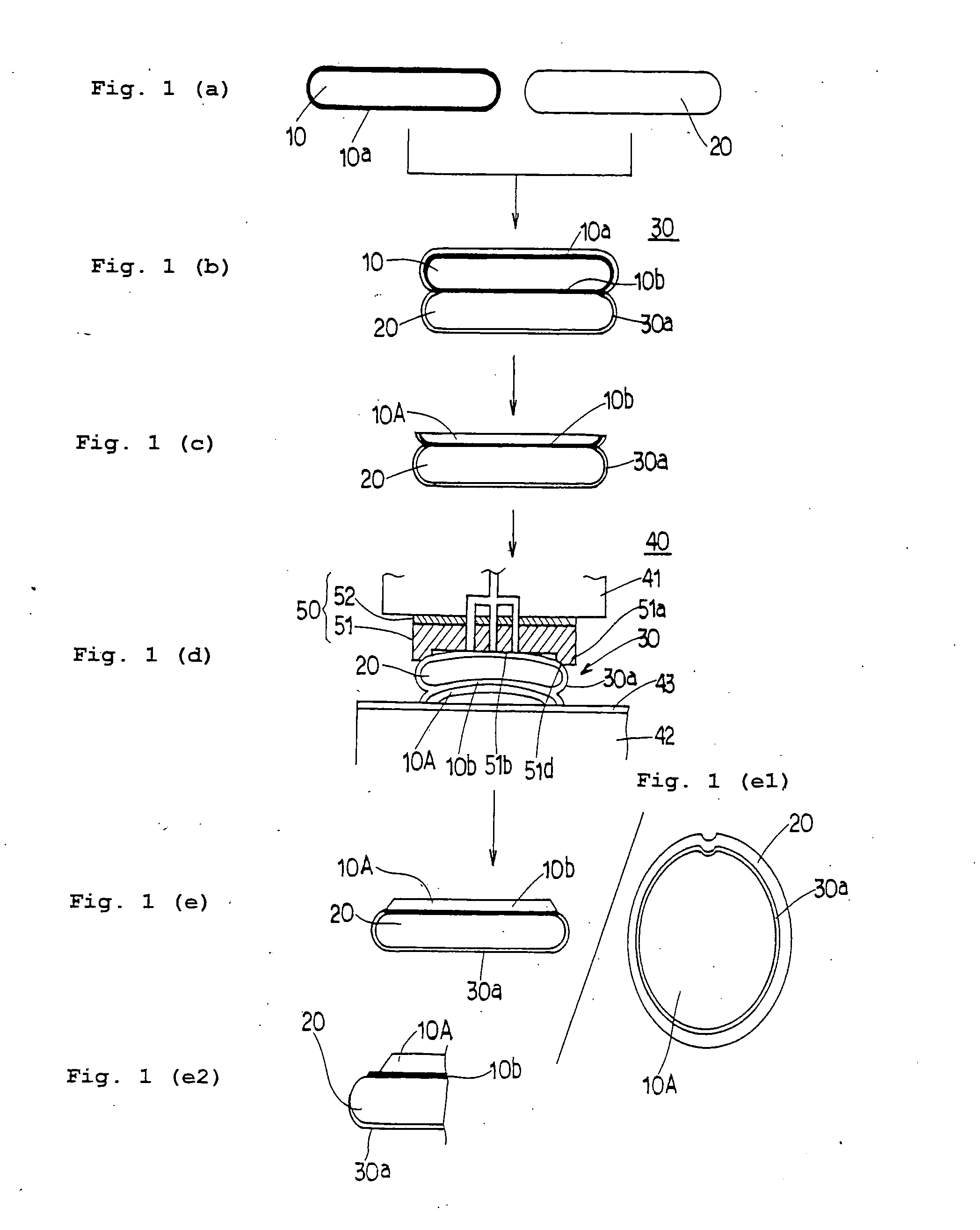
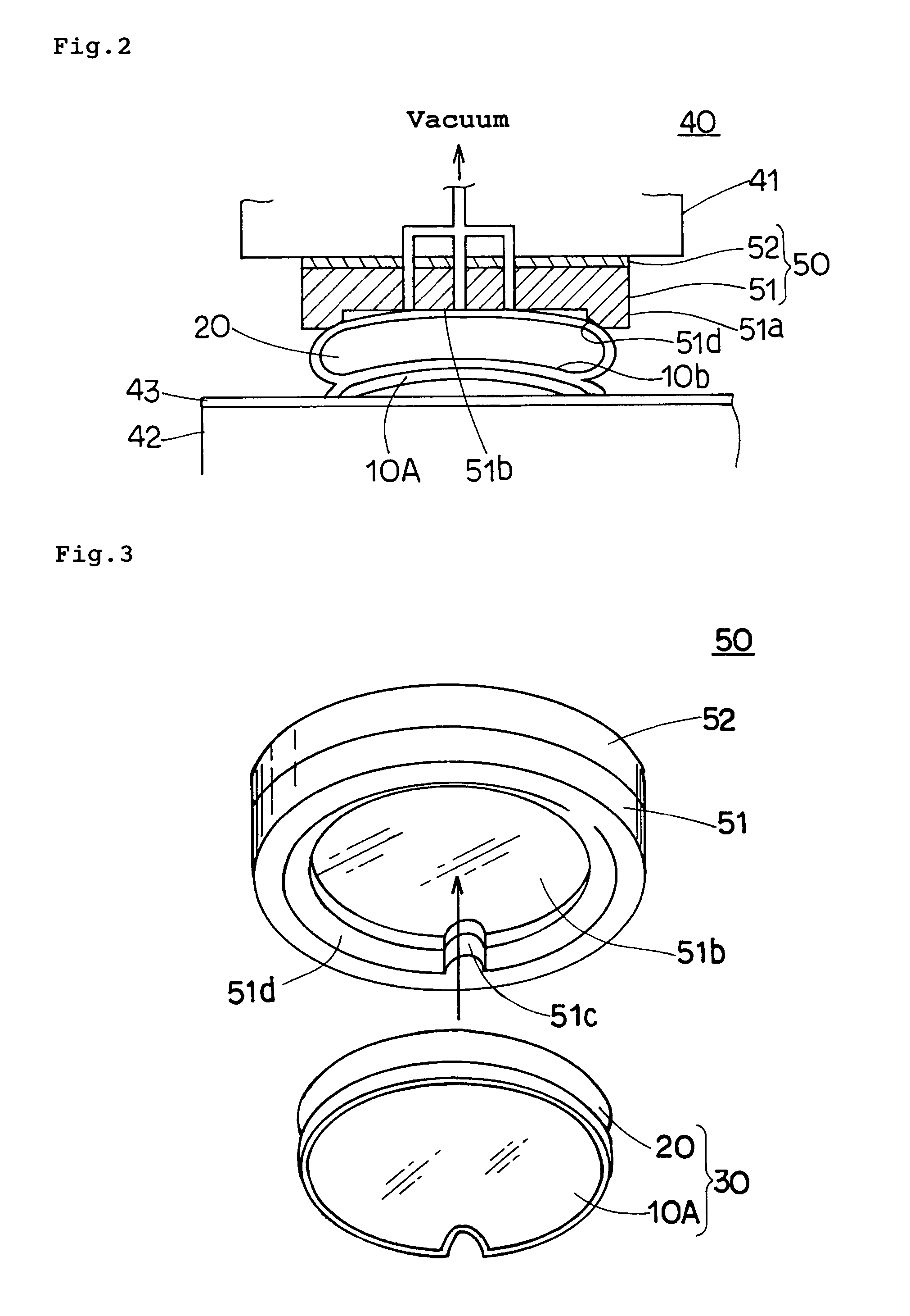
[0153] Preferred embodiments of the present invention will now be described with reference to the attached drawings. It is to be appreciated that the present invention is not limited to those embodiments. First of all, referring to FIG. 1 through FIG. 16, a first embodiment will be described.

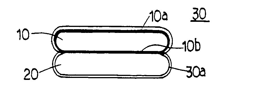
[0154] As shown in FIG. 1, first of all, a single crystal silicon ingot is pulled up by using the Czochralski method, and then thus obtained single crystal silicon ingot is applied to a series of processing consisting of block cutting, notch processing, slicing, beveling, lapping, etching and mirror polishing to prepare a mirror finished active layer wafer 10 with a notch having a thickness of 725 μm and a diameter of 200 mm. On the other hand, by using the same production processes as those applied to this active layer wafer 10, a mirror finished supporting substrate wafer 20 with notch having the same thickness and the same diameter therewith is prepared (FIG. 1(a)). It is to be noted that the...

second embodiment

[0185] the present invention will now be described with reference to FIG. 17 through FIG. 22.

[0186] The feature of the second embodiment resides in a point that after the periphery removing polishing in the first embodiment, a partial periphery removing polishing process is applied, in which only a portion in the circumferential direction of the peripheral region of the bonding wafer 30 is polished again (i.e., the second polishing) so as to remove the active layer 10A in that portion.

[0187] A specified portion of the bonding wafer 30 subject to the second polishing is the portion in the vicinity of the orientation flat. By applying such a partial periphery removing polishing, a width, d, of a terraced section in the vicinity of the orientation flat of the supporting substrate wafer 20 is extended, and the hard laser mark, M, may be printed on that extended terraced section (FIG. 19). For partial periphery removing polishing, a partial wafer removing pressing jig 60 is used.

[0188]...


PUM


Abstract

Provided are a bonding substrate whose defective bonding portion in a peripheral region of an active layer has been removed by a polishing applied thereto after a surface grinding, a manufacturing method of the same substrate and wafer periphery pressing jigs. After the surface grinding, a periphery removing polishing is applied from an active layer wafer side of a bonding wafer so that a peripheral region of the active layer may be removed and a central region thereof may be left un-removed. Consequently, a periphery grinding and a periphery etching according to the prior art can be eliminated. Furthermore, an etch pit on a circumferential face of a wafer which could be caused by the periphery etching and a contamination or a scratching in an SOI layer which could be caused by a silicon oxide film left un-ground-off can be prevented, thereby achieving high yield and low cost.

Description

FIELD OF THE INVENTION [0001] The present invention relates to a bonding substrate, a method for manufacturing the same and a wafer periphery pressing jig used in the same method, and in more specific, to a technology for manufacturing a bonding substrate, in which, for example, a removal processing of a defective bonding portion in a peripheral region of an active layer is carried out in a polishing process after a surface grinding. DESCRIPTION OF THE PRIOR ART [0002] One known type of the bonding substrate comprising two pieces of silicon wafers that have been bonded in one on the other includes a bonding SOI (Silicon on Insulator) substrate. This represents the bonding SOI substrate comprising an oxide film (silicon oxide film) of some μm thick implanted between an SOI layer (active layer) on a surface of which a device is to be formed and a supporting substrate wafer which supports the SOI layer from a back side thereof. [0003] One method has been known for manufacturing this ty...

Claims


Application Information

Patent Timeline
IPC IPC(8): H01L21/00H01L21/68H01L21/762
CPCH01L21/76251B24B37/30H01L21/20
Inventor TOMITA, SHINICHIYOSHIMARU, KOUJI
Owner SUMITOMO MITSUBISHI SILICON CORP
Why Eureka
Try Eureka