Substrate holder and plating apparatus

Active Publication Date: 2005-01-20
EBARA CORP
View PDF13 Cites 55 Cited by
  • Summary
  • Abstract
  • Description
  • Claims
  • Application Information

AI Technical Summary

Benefits of technology

[0013] The present invention has been made in view of the above situation in the prior art. It is therefore a first object of the present invention to provide a substrate holder which can e

Problems solved by technology

According to the dipping method of electroplating, bubbles that can adversely affect the quality of the plating are easily removed and the footprint is small.
Due to deterioration of sealing member, etc., however, it is difficult to effect a complete sealing.
Complete sealing is difficult especially in carrying out plating to embed a plated film into fine recesses, since a plating solution having a good permeability is generally used in such a plating so that the plating solution can easily and fully permeate into the fine recesses.
On the other hand, it is also generally difficult to detect a leak of plating solution or other liquid.
Once a leak of plating solution occurs, the plating solution, which has leaked into a substrate holder, adheres to the back surface of a substrate, and the plating solution adhering to the substrate will transfer to

Method used


Image

  • Substrate holder and plating apparatus
  • Substrate holder and plating apparatus
  • Substrate holder and plating apparatus

Examples


Embodiment Construction

[0111] Preferred embodiments of the present invention will now be described with reference to the drawings.

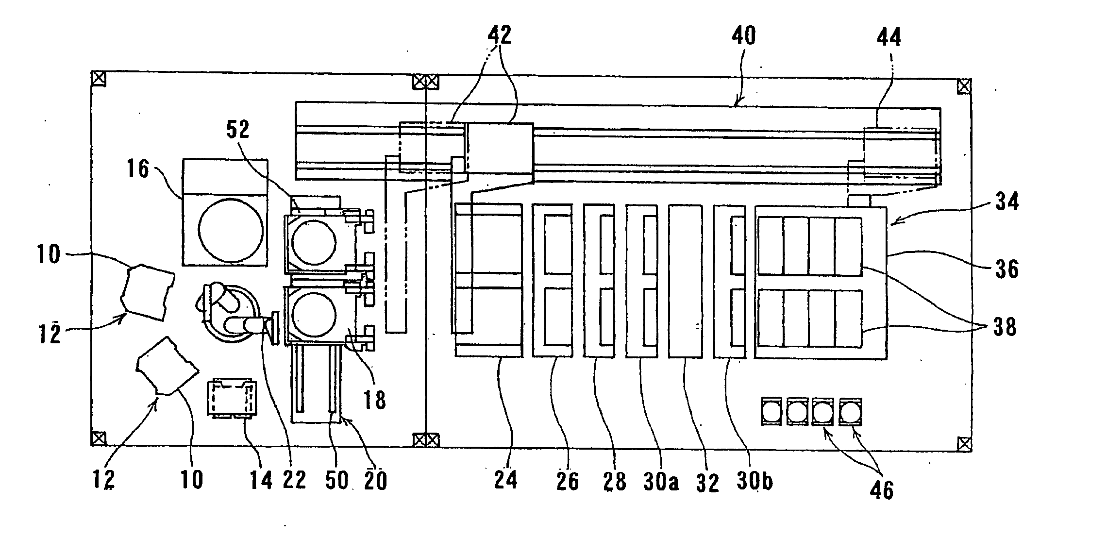
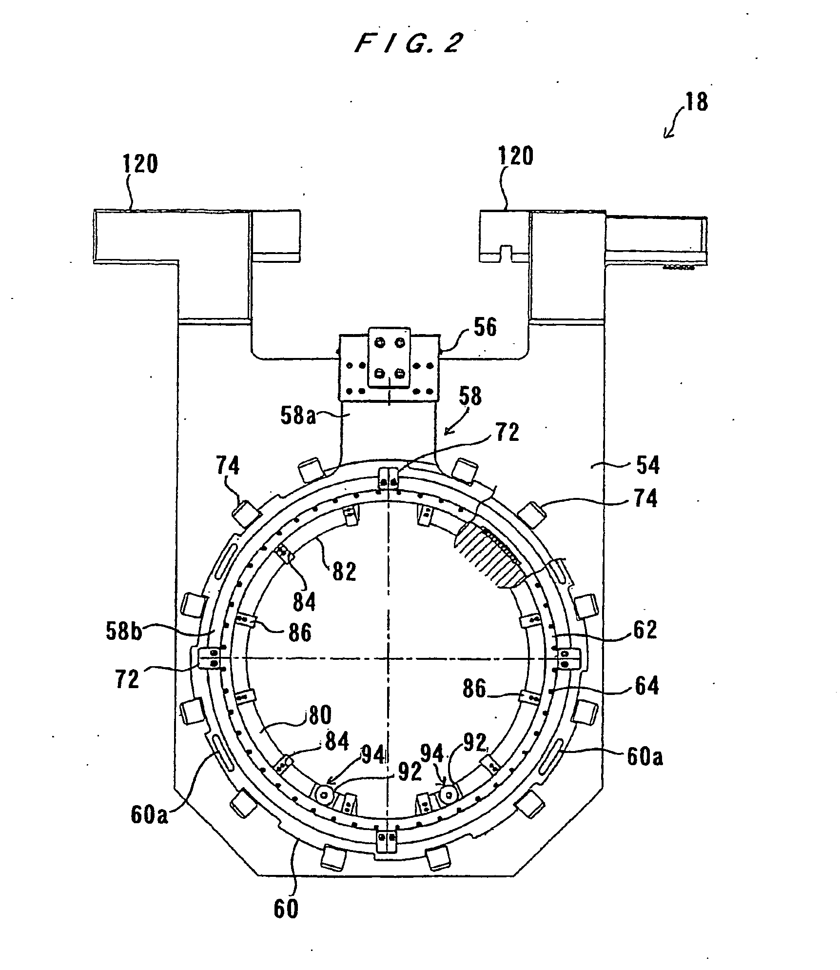
[0112]FIG. 1 shows a layout plan of a plating apparatus provided with a substrate holder according to an embodiment of the present invention. As shown in FIG. 1, the plating apparatus includes two cassette tables 12 each for placing thereon a cassette 10 for housing substrates W such as semiconductor wafers, an aligner 14 for aligning the position of an orientation flat or a notch of the substrate W in a predetermined direction, and a spin drier 16 for rotating the substrate W after plating at a high speed to dry the substrate. Further, a substrate attaching / detaching section 20 for placing thereon a substrate holder 18 for detachably holding the substrate W, and attaching / detaching the substrate W to / from the substrate holder 18, is provided near the spin drier 16. Furthermore, a substrate transfer device 22, comprised of a transfer robot, is disposed in the center of the abo...


PUM

PropertyMeasurementUnit
Electric energyaaaaaaaaaa
Forceaaaaaaaaaa
Pressureaaaaaaaaaa

Abstract

The present invention is to provide a substrate holder which can effect a more complete sealing with a sealing member and makes it possible to take a substrate out of it easily and securely, and also a plating apparatus provided with the substrate holder. A substrate holder (18), includes: a fixed holding member (54) and a movable holding member (58) for holding a substrate (W) therebetween; a sealing member (68) mounted to the fixed holding member (54) or the movable holding member (58); and a suction pad (94) for attracting a back surface of the substrate (W) held between the fixed holding member (54) and the movable holding member (58).

Description

TECHNICAL FIELD [0001] The present invention relates to a substrate holder for use in a plating apparatus for plating a to-be-plated surface of a substrate, especially a plating apparatus for forming a plated film in fine interconnect trenches or holes, or resist openings provided in the surface of a semiconductor wafer, or for forming bumps (protruding electrodes), which are to be electrically connected to electrodes, etc. of a package, on the surface of a semiconductor wafer, and also to a plating apparatus provided with the substrate holder. BACKGROUND ART [0002] In a tape automated bonding (TAB) or flip chip, for example, it has been widely conducted to deposit gold, copper, solder, nickel or multi-layered materials thereof at prescribed areas (electrodes) on the surface of a semiconductor chip having interconnects, thereby forming protruding connecting electrodes (bumps). Such bumps electrically connect the semiconductor chip with package electrodes or TAB electrodes. There are...

Claims


Application Information

Patent Timeline
IPC IPC(8): C25D7/12C25D17/06C25D17/08H01L21/00H01L21/288H01L21/60H01L21/687
CPCC25D17/06C25D7/12H01L21/67126H01L21/68728H01L21/68764H01L24/11H01L2224/13099H01L2924/01002H01L2924/01013H01L2924/01022H01L2924/01027H01L2924/01029H01L2924/01033H01L2924/01047H01L2924/01051H01L2924/01074H01L2924/01078H01L2924/01079H01L2924/01082H01L2924/01006H01L2924/01023H01L2924/014H01L2924/01005C25D7/123C25D17/001H01L21/2885H01L2224/05573H01L2224/05568H01L2924/00014H01L2224/05599H01L21/68H01L21/288H01L21/02C25D17/004C25D17/005C25D17/08C25D21/12H01L21/67253H01L21/6838H01L21/687H01L21/76879H01L24/742H01L2224/11462H01L2224/13139H01L2224/13144H01L2224/13147H01L2224/13155H01L2224/13169H01L2924/01028
Inventor YOSHIOKA, JUNICHIROHORIE, KUNIAKIGUO, YUGANGMORIKAMI, SATOSHI
Owner EBARA CORP
Why Eureka
Try Eureka