Cleaning process and apparatus for silicate materials

a silicate material and cleaning process technology, applied in the direction of coatings, decorative arts, chemical vapor deposition coatings, etc., can solve the problems of reducing the “yield” of usable devices, loose particles of these polymers may break off, contaminating the wafer, etc., to reduce cracks, fractures and other defects, increase the stiction of contaminant layers, and increase surface area

Inactive Publication Date: 2005-01-27
QUANTUM GLOBAL TECH
View PDF51 Cites 10 Cited by
  • Summary
  • Abstract
  • Description
  • Claims
  • Application Information

AI Technical Summary

Benefits of technology

[0013] The present invention provides methods and apparatus for treating silicon-containing materials and, in particular, textured quartz. The present invention provides a high surface area (as preferably measured by roughness), which increases the stiction of contaminant layers to the textured quartz working surface. Furthermore, the present invention reduces cracks, fractures and other defects in the textured quartz surface, thereby reducing contaminant particles that may flake off or otherwise be dislodged from the quartz surface.

Problems solved by technology

Such contaminants can damage the wafer, reducing the “yield” of usable devices.
Loose particles of these polymers may break off during the manufacturing process and contaminate the wafers.
Contaminants can cause high resistance, adhesion problems for subsequent layers, reduced insulation, and other performance and reliability problems.
Sometimes, when manual scrubbing is not thorough enough, the yield of semiconductors subsequently processed will be greatly affected.
Furthermore, scrubbing does not tend to be completely thorough, especially with high-surface area textured surfaces.
However, the prior art methodology is generally not well suited for cleaning processing chambers which include quartz substrates.
Quartz parts and domes are frequently sent out to specialty cleaning houses or replaced, at considerable cost.
However, contaminants which may be deposited on quartz of such smoothness during the semiconductor manufacturing process do not adhere well to the quartz surface, and are prone to becoming separated from the quartz surface and settling on the semiconductor wafer being processed.
If the angle is less steep than about 60°, the texturing process is considered to be too slow for most purposes.
However, it has been found that grit-blasting at the high angles tends to create cracks 150 in the roughened surface.
Such particle contaminants may introduce impurities in the wafers being processed, adversely affect yield.

Method used


Image

  • Cleaning process and apparatus for silicate materials
  • Cleaning process and apparatus for silicate materials
  • Cleaning process and apparatus for silicate materials

Examples


Embodiment Construction

[0032] Unless otherwise indicated, all technical and scientific terms used herein have the same meaning as they would to one skilled in the art of the present invention. It is to be understood that this invention is not limited to the particular methodology, protocols and reagents described, as these may vary. All publications and patents cited herein are expressly incorporated herein by reference for the purpose of describing and disclosing methodologies and devices with might be used in connection with the cleaning and micro-roughing processes and devices of the invention.

[0033] I. Definitions

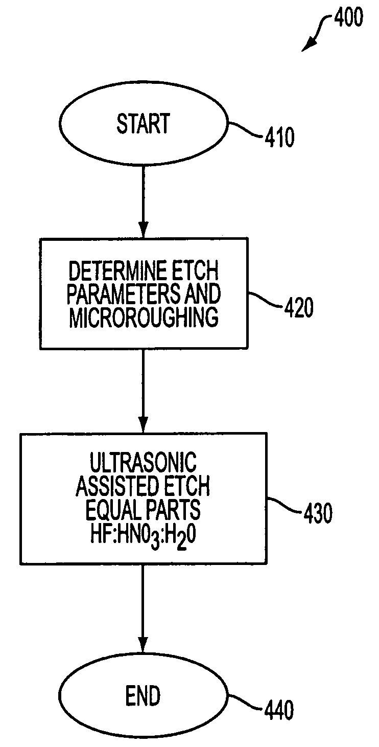
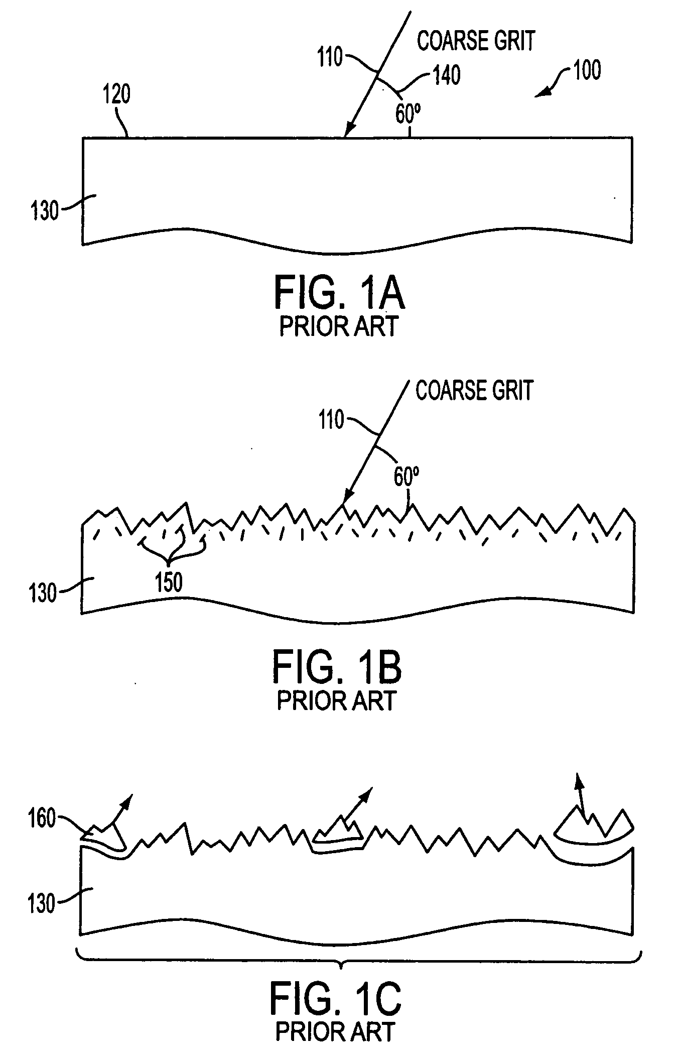
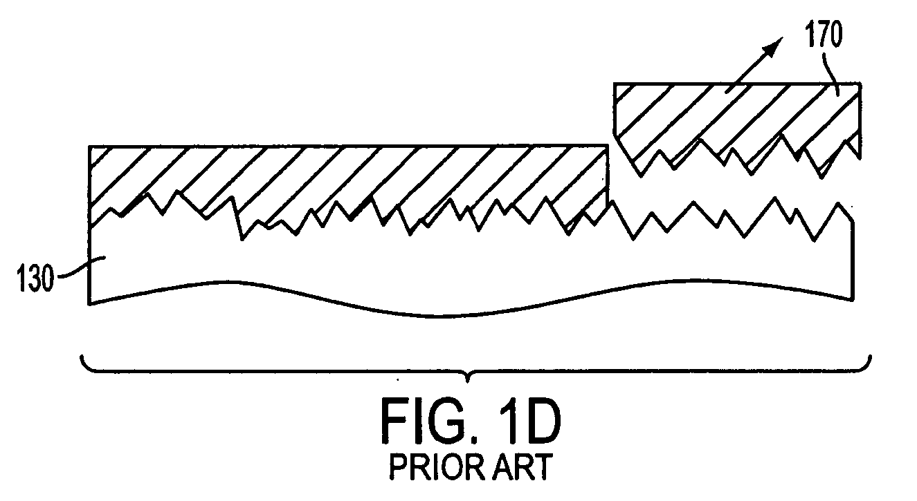
[0034] By “micro-roughening” or “micro-roughness” is meant the root mean square of the short-range deviations of a surface above and below its mean position, and includes the way in which the micro-roughness is distributed at different spatial frequencies, or different sizes, of structure on the surface of interest. This is to be distinguished from isolated surface defects and contaminants ...


PUM

PropertyMeasurementUnit
angleaaaaaaaaaa
distanceaaaaaaaaaa
distanceaaaaaaaaaa

Abstract

A method for treating a surface of a quartz substrate includes preparing a substrate to provide a working surface having an initial roughness; and then ultrasonically acid-etching the working surface to increase the roughness of the working surface by at least about 10%. In one embodiment, the initial surface roughness is greater than about 10 Ra, and in another embodiment the initial surface roughness is greater than about 200 Ra. In a still further embodiment, the initial surface area, if less than about 200 Ra, is increased to greater than about 200 Ra. In other embodiments of the present invention, the working surface roughness is increased by at least about 25% or at least about 50%. Simultaneous with the increase in surface area (as measured by the roughness), the surface defects are reduced to reduce particulate contamination from the substrate.

Description

CROSS-REFERENCE TO RELATED APPLICATIONS [0001] This application is related to co-owned and copending U.S. patent application Ser. No. ______ (attorney reference 59081-8007.US01), entitled “Ultrasonic Assisted Etch Using Corrosive Liquids”, filed concurrently herewith, and incorporated herein by reference in its entirety.BACKGROUND OF THE INVENTION [0002] 1. Field of the Invention [0003] The present invention relates to methods and apparatus for treating silicate substrate surfaces and, more particularly, textured quartz substrates. [0004] 2. Description of the Related Art [0005] During most semiconductor manufacturing processes, such as dielectric etching or chemical vapor deposition, unwanted materials are sometimes formed on the interior surfaces of the processing chamber and on the chamber parts used in the manufacturing process. It is important that the materials deposited on the interior surfaces and chamber parts not become a source of contaminants that can flake, fall, or be ...

Claims


Application Information

Patent Timeline
Patent Type & Authority Applications(United States)
IPC IPC(8): B44C1/22C23C16/44C23F1/00H01L
CPCC23C16/4407C23C16/4404C23F1/00
Inventor TAN, SAMANTHA S. H.CHEN, NING
Owner QUANTUM GLOBAL TECH
Why Eureka
Try Eureka