Residual gas analyzer of semiconductor device manufacturing equipment

a gas analyzer and semiconductor device technology, applied in the direction of instruments, particle separator tube details, separation processes, etc., can solve the problems of damage to the vacuum system of the apparatus, and defects can be produced in the wafers that are being processed, so as to prevent the defect of the products being processed in the process chamber and the accuracy of detection

Inactive Publication Date: 2005-01-27
SAMSUNG ELECTRONICS CO LTD
View PDF9 Cites 5 Cited by
  • Summary
  • Abstract
  • Description
  • Claims
  • Application Information

AI Technical Summary

Benefits of technology

[0016] An object of the present invention is to provide a residual gas analyzing apparatus of semiconductor manufacturing equipment that operates in step with the process cha

Problems solved by technology

Furthermore, condensation may occur and thus damage the vacuum system of the apparatus.
Thus, if the technician does not

Method used


Image

  • Residual gas analyzer of semiconductor device manufacturing equipment
  • Residual gas analyzer of semiconductor device manufacturing equipment
  • Residual gas analyzer of semiconductor device manufacturing equipment

Examples


Embodiment Construction

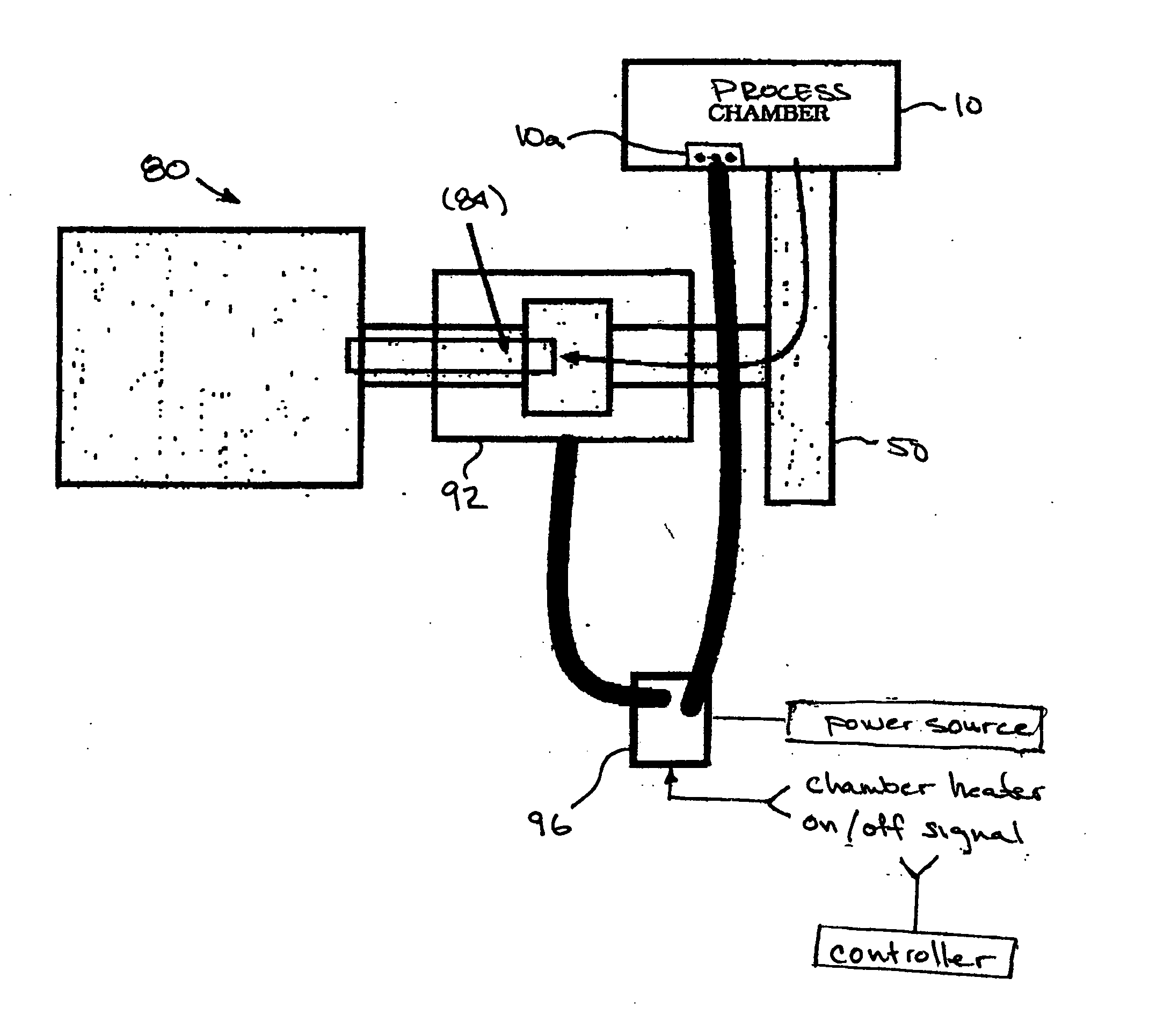
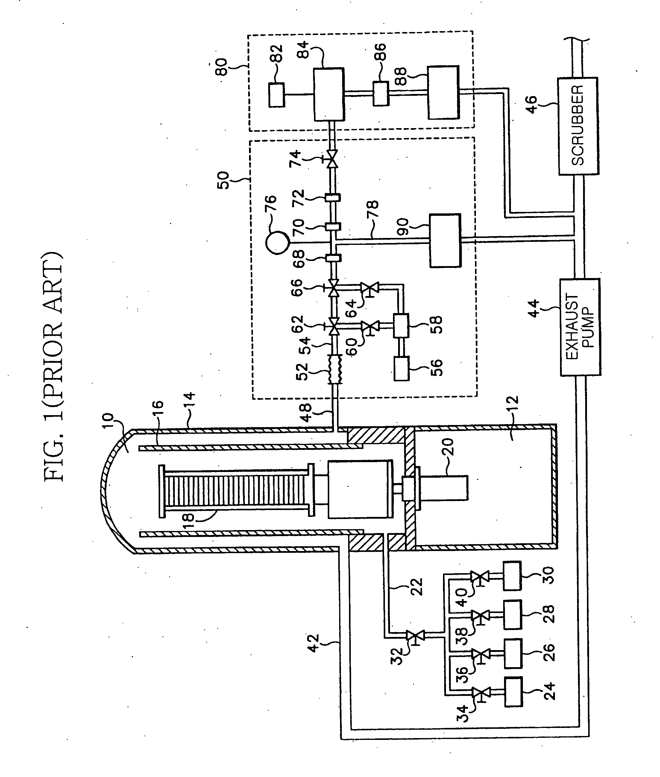
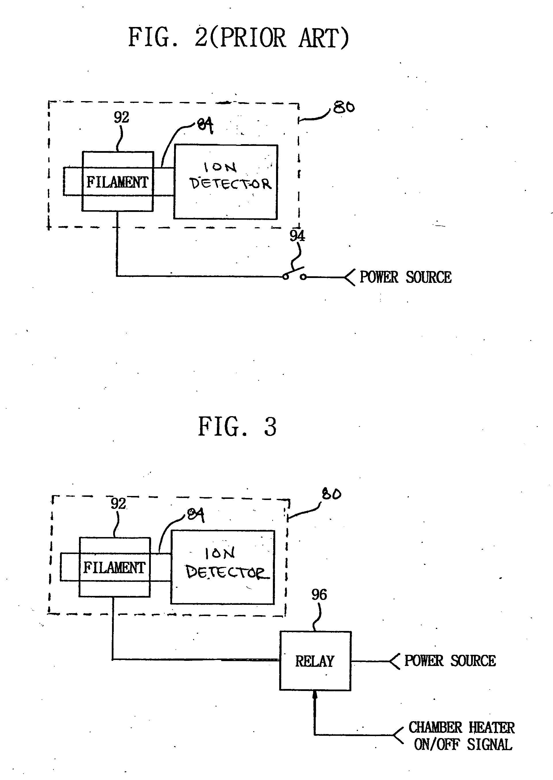
[0026] The present invention will be described in detail with reference to FIGS. 3 and 4. It will be understood that many of the details of the present invention have already described in connection with the chemical vapor deposition apparatus shown in FIG. 1. Thus, a detailed description of the known functions and systems of the apparatus will not be repeated in the detailed description that follows.

[0027] Turning now to FIGS. 3 and 4, the heating system of a residual gas analyzer 80 according to the present invention includes a heater 92, comprising a filament and a heating jacket, and a relay 96. The relay 96 operates in response to an on / off signal supplied to a process chamber 10 to initiate a baking process. The operation of the heating system will be described in more detail below.

[0028] The chemical vapor deposition apparatus has a main power source for operating the heater 10a of the process chamber 10. A chamber heater “on signal” is generated by a controller of the chem...


PUM

PropertyMeasurementUnit
Poweraaaaaaaaaa
Compositionaaaaaaaaaa

Abstract

In semiconductor manufacturing equipment having a residual gas analyzing apparatus for analyzing the composition of residual gas in a process chamber of the equipment, a heater of the residual gas analyzer is interlocked with a heater of the process chamber. The residual gas analyzer includes an ion detector, and the heater of the residual gas analyzer has a filament and a heating jacket surrounding a portion of the ion detector. A relay connects a power source of the heater for the process chamber to the heater of the residual gas analyzer. Power is supplied to and cut off from the heater of the residual gas analyzer in response to heater on/off signals used for controlling the operation for the heater for the process chamber.

Description

BACKGROUND OF THE INVENTION [0001] 1. Field of the Invention [0002] The present invention relates to a chemical vapor deposition apparatus for use in manufacturing a semiconductor device. More particularly, the present invention relates to a gas analyzing apparatus for analyzing the residual gas in the reaction chamber of a chemical vapor deposition apparatus. [0003] 2. Description of the Related Art [0004] A semiconductor device is generally manufactured by selectively and repeatedly subjecting a wafer to a number of processes such as photolithography, etching, diffusion, chemical vapor deposition, ion implantation and metal deposition processes. The etching, diffusion and chemical vapor deposition processes are performed by supplying a process gas into a sealed process chamber, and by providing an atmosphere in the chamber that facilitates a reaction between the process gas and the wafer. Accordingly, a gaseous by-product of the reaction, as well as unreacted process gas, remain i...

Claims


Application Information

Patent Timeline
IPC IPC(8): C23C16/52H01L21/205G01M3/04H01J49/04
CPCH01J49/00C23C16/52H01L21/205
Inventor KIM, SEON-WOO
Owner SAMSUNG ELECTRONICS CO LTD
Why Eureka
Try Eureka