Silicon on diamond wafers and devices

a technology of silicon and diamond, applied in the direction of semiconductor devices, semiconductor/solid-state device details, electrical equipment, etc., can solve the problems of failure of components, power consumption and package size declines, and circuit density and complexity increases

Inactive Publication Date: 2005-01-27
INTEL CORP
View PDF7 Cites 94 Cited by
  • Summary
  • Abstract
  • Description
  • Claims
  • Application Information

AI Technical Summary

Problems solved by technology

The semiconductor industry has seen tremendous advances in technology in recent years that have permitted dramatic increases in circuit density and complexity, and equally dramatic decreases in power consumption and package sizes.
If the heat generated is not removed from the component, the heat produced can drive the temperature of the component to levels that result in failure of the component.
In some instances, the full capability of certain components can not be realized since the heat the component generates at the full capability would result in failure of the component.
Furthermore, as computer related equipment becomes smaller and more powerful, more components are being used as part of one piece of equipment.
There is generally a limitation on the amount of heat that can be extracted from the back side of the integrated circuit or die, because of the thermal resistance induced by the thermal interface materials (such as a silicon die, a heat pipe to transport heat from the die to the heat sink, and any thermal grease or adhesives) used between the back side of the integrated circuit die and the heat sink.
The materials used currently as heat sinks have a limited ability to conduct heat.
The use of aluminum and copper heat sinks with fin structures are now approaching their practical limits for removal of heat from a high performance integrated circuit, such as the integrated circuits that include dies for microprocessors.
When heat is not effectively dissipated, the dies develop “hot spots” or areas of localized overheating.
Ultimately, the circuitry within the die fails.
When the die fails, the electrical component also fails.
Diamond heat sinks are difficult to manufacture and expensive.
Grinding or smoothing diamond is time consuming.

Method used


Image

  • Silicon on diamond wafers and devices
  • Silicon on diamond wafers and devices
  • Silicon on diamond wafers and devices

Examples


Embodiment Construction

[0025] In the following detailed description of the preferred embodiments, reference is made to the accompanying drawings that form a part hereof, and in which are shown by way of illustration specific embodiments in which the invention can be practiced. The embodiments illustrated are described in sufficient detail to enable those skilled in the art to practice the teachings disclosed herein. Other embodiments can be utilized and derived therefrom, such that structural and logical substitutions and changes can be made without departing from the scope of present inventions. The following detailed description, therefore, is not to be taken in a limiting sense, and the scope of various embodiments of the invention is defined only by the appended claims, along with the full range of equivalents to which such claims are entitled.

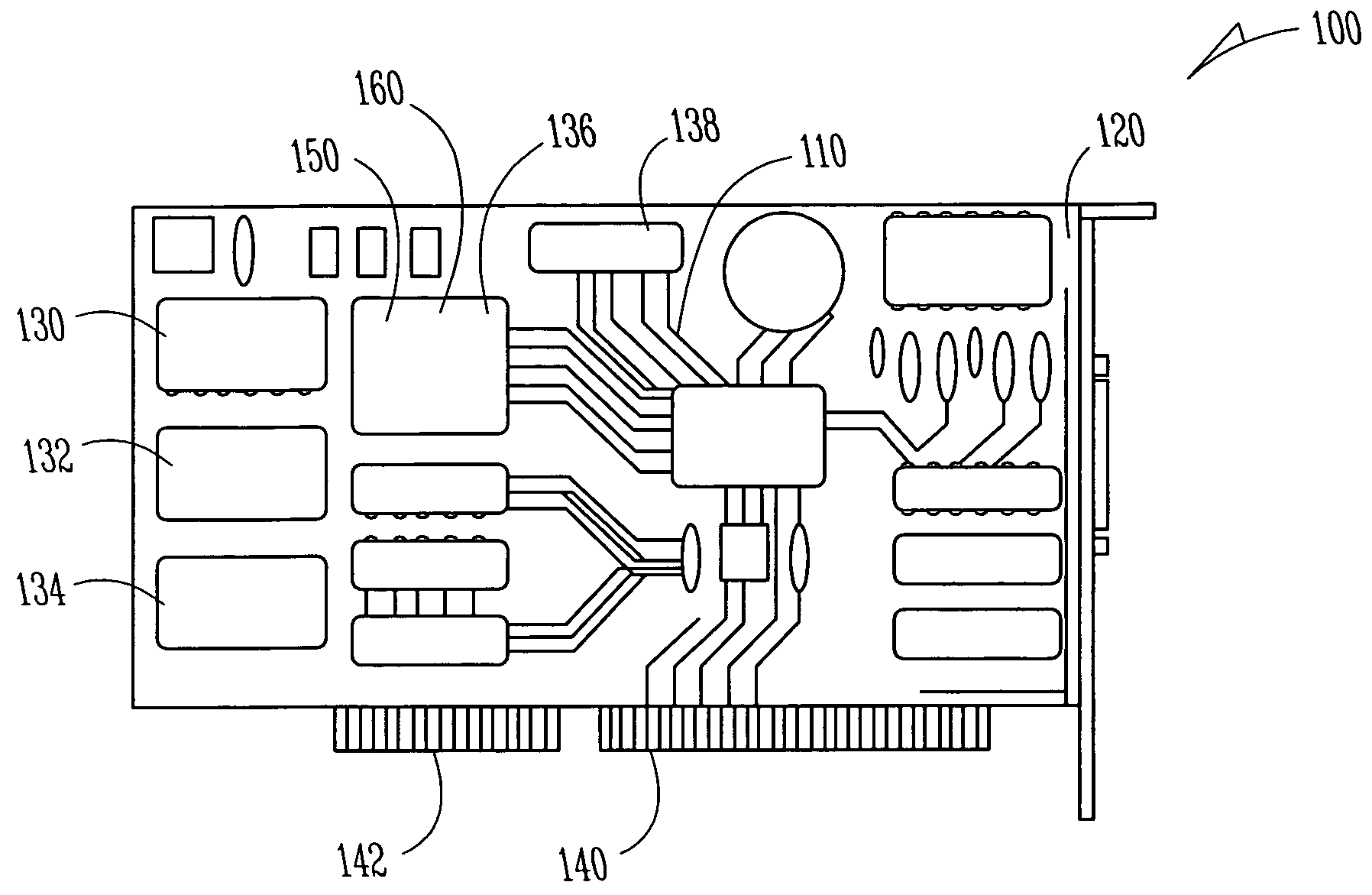
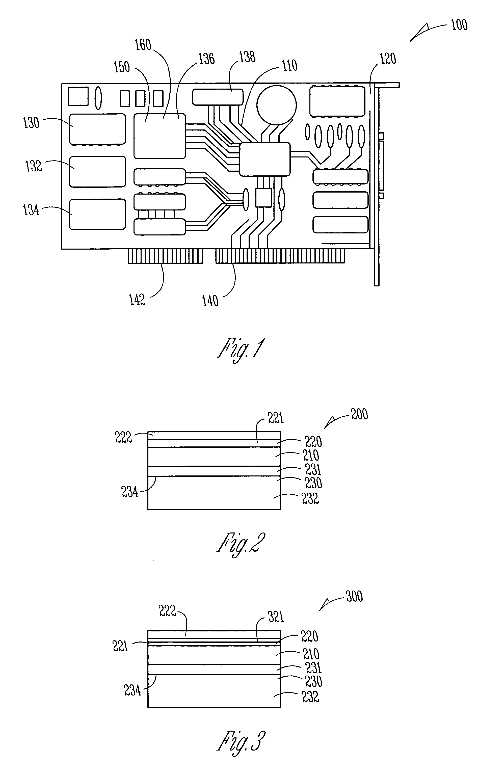
[0026]FIG. 1 is a top view of a printed circuit board 100, having a component with a die having a buried diamond layer, according to an embodiment of the inven...


PUM

PropertyMeasurementUnit
thicknessaaaaaaaaaa
thicknessaaaaaaaaaa
thicknessaaaaaaaaaa

Abstract

A heat dissipation device includes a first silicon layer, a second silicon layer, and a diamond layer sandwiched between the first silicon layer and the second silicon layer. A method for forming an electronic device includes sandwiching a layer of diamond between a first layer of silicon and a second layer of silicon, and forming an electrical device on one of the first layer of silicon or the second layer of silicon. The method further includes forming an epitaxial layer on one of the first layer of silicon and the second layer of silicon. An electrical device is formed in the epitaxial layer.

Description

FIELD OF THE INVENTION [0001] The present invention is related to a heat dissipation system for a wafer which is cut into individual dies. More specifically, the present invention relates to a silicon on diamond wafers and devices and the manufacture of the same. BACKGROUND OF THE INVENTION [0002] The semiconductor industry has seen tremendous advances in technology in recent years that have permitted dramatic increases in circuit density and complexity, and equally dramatic decreases in power consumption and package sizes. Present semiconductor technology now permits single-chip microprocessors with many millions of transistors, operating at speeds of tens (or even hundreds) of MIPS (millions of instructions per second), to be packaged in relatively small, air-cooled semiconductor device packages. As integrated circuit devices, microprocessors and other related components are designed with increased capabilities and increased speed, additional heat is generated from these component...

Claims


Application Information

Patent Timeline
Patent Type & Authority Applications(United States)
IPC IPC(8): H01L23/373
CPCH01L23/3732H01L2924/0002H01L2924/00
Inventor RAVI, KRAMADHATI V.
Owner INTEL CORP
Why Eureka
Try Eureka