Laminated polymer optical waveguide and process for producing the same

a technology of laser-cutting polymer and optical waveguide, which is applied in the direction of optical waveguide light guide, instruments, applications, etc., can solve the problems of poor cost performance, inability to obtain sufficient difference in refractive index between the core layer and the clad layer, and poor accuracy of a core diameter. , to achieve the effect of reducing connection loss, facilitating positioning, and reducing cos

Inactive Publication Date: 2005-01-27
FUJIFILM BUSINESS INNOVATION CORP
View PDF5 Cites 40 Cited by
  • Summary
  • Abstract
  • Description
  • Claims
  • Application Information

AI Technical Summary

Benefits of technology

[0022] An object of the invention is to provide a laminated polymer optical waveguide wherein an optical waveguide core belonging to any one of laminated layers can be freely arranged, and a process for producing a laminated polymer optical waveguide at a low cost and in a simple process.
[0039] According to the laminated polymer optical waveguide of the invention, even if the light-transmissive films that are used have varying thicknesses, the flexibility of the optical waveguide films allows easy positioning in the direction along which the optical waveguide films are laminated (i.e., in the lamination direction). Therefore, the optical waveguide of the invention has an advantage in that it can be connected to an optical connector at lower costs and with a lower connection loss as compared with optical waveguides having other structures and optical fiber laid substrates. An optical waveguide core belonging to any one of the laminated layers can be freely arranged and led to the optical connector.
[0040] Further, the process for producing a laminated polymer optical waveguide of the invention has very simple steps. Accordingly, the laminated polymer optical waveguide can be easily produced. Thus, the laminated polymer optical waveguide can be produced at far lower costs as compared with conventional processes for producing a laminated polymer optical waveguide. According to the process of the invention, a flexible laminated polymer optical waveguide which exhibits only a small amount of loss, has a high precision and can be freely mounted to various devices can be obtained. Furthermore, the shape and the like of the laminated polymer optical waveguide can be freely set.

Problems solved by technology

However, the selective polymerization method (1) has a problem concerning the adhesion of the film, and the methods (2) and (3) are poor in cost performance as they employ photolithography.
The method (4) has a problem concerning the accuracy of a core diameter.
Also, the method (5) has the problem that a sufficient difference in refractive index between the core layer and the clad layer cannot be obtained.
However, these methods have a cost problem as mentioned above.
Also, any of the methods (1) to (5) is not applicable to the formation of a polymer optical waveguide on a flexible plastic substrate having a large area.
However, in this method, there is the problem that the polymer precursor material is not only filled in the capillary groove but also filled thinly in the entire space between the patterned substrate and the plane substrate, the polymer precursor material applied between both substrates is cured to form a thin layer having the same composition as the core layer, resulting in that light leaks through this thin layer.
However, since this method uses a monomer as the core-forming material, it has the problem that the volume shrinkage factor when the monomer is polymerized into a polymer is large and the transmission loss of the polymer optical waveguide is increased.
Also, this method is such a complicated method that the patterned substrate is fixed with the plane substrate by a clamp and in addition to this process, the contact part is sealed with a resin, and is therefore unfit for mass-production, with the result that no reduction in cost can be expected.
Also, it is impossible to apply this method to the production of a polymer optical waveguide using a film having a thickness of the order of millimeters or 1 mm or less as a clad.
However, even if the production method described in this patent is applied to the production of a polymer optical waveguide, a lot of time is required to form a core part because the core part of the optical waveguide has a small sectional area, showing that this method is not suitable to mass-production.
This method also has the drawback that a change in volume is caused when the monomer solution is polymerized to form a polymer, leading to a change in the shape of the core with a large transmission loss.
However, if an optical waveguide is produced using such a micro-mold method as aforementioned, it is not impossible to make volume shrinkage factor small during curing (hence making transmission loss small) and to drop the viscosity of a filler liquid (monomer or the like) to make it easy to fill at the same time.
Therefore, the viscosity of the filler liquid cannot be dropped to a certain limit or less, leading to a small filling speed and therefore mass-production is not expected taking it account preferentially to make transmission loss small.
It is difficult to form optical waveguide cores in a film-penetrating direction, and thus it has been difficult to lead optical waveguide cores belonging to different laminated layers to, for example, an optical connector whose cores are arranged along a straight line at regular intervals, such as an MT connector.
However, the flexibility of the arrangement of the optical waveguide cores is limited.
For example, it is impossible to select only some optical waveguide cores from among the optical waveguide cores in an end face of the laminated layers, and arrange the sections of the selected optical waveguide cores along a straight line at regular intervals.

Method used


Image

  • Laminated polymer optical waveguide and process for producing the same
  • Laminated polymer optical waveguide and process for producing the same
  • Laminated polymer optical waveguide and process for producing the same

Examples


example 1

[0143]

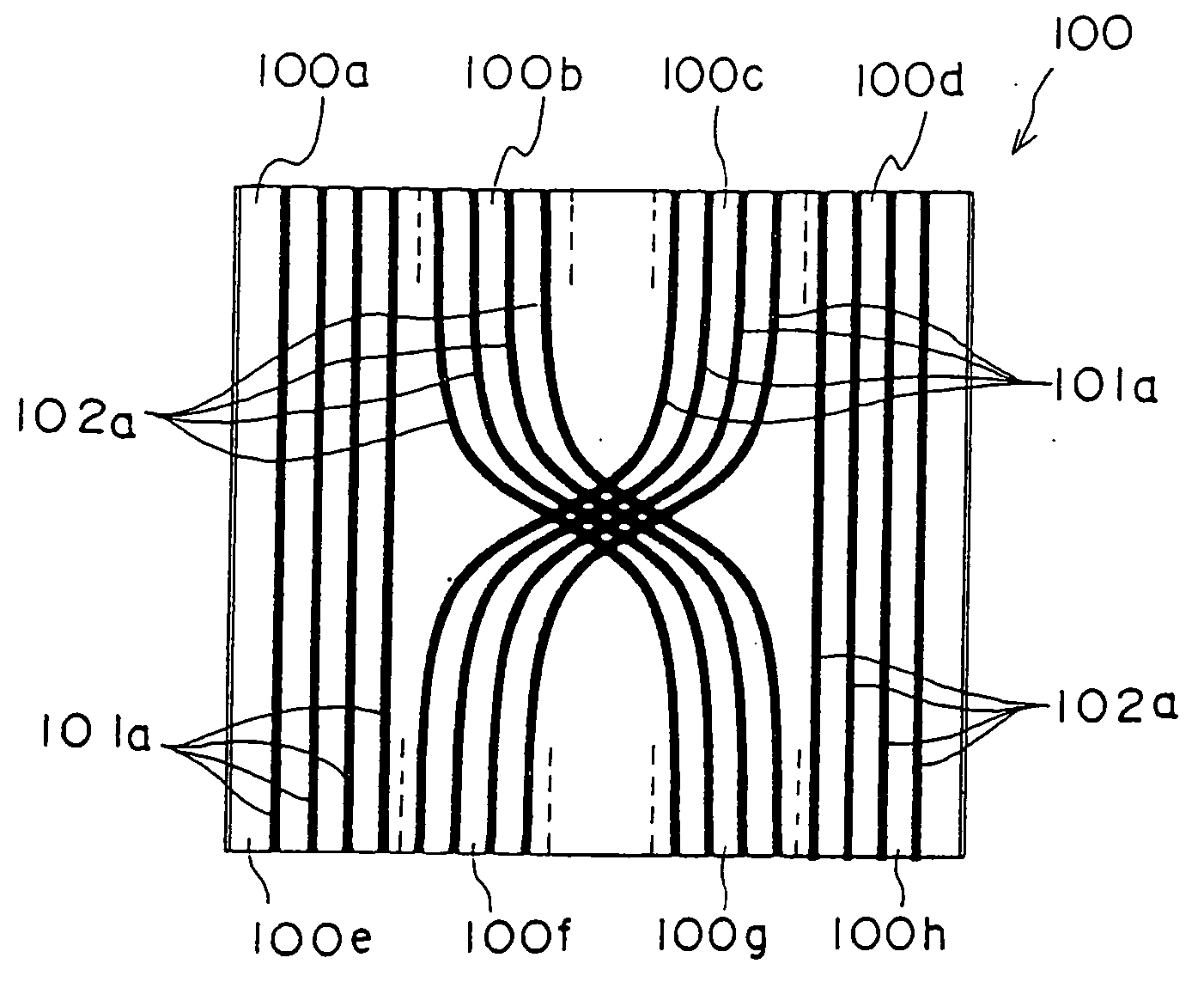
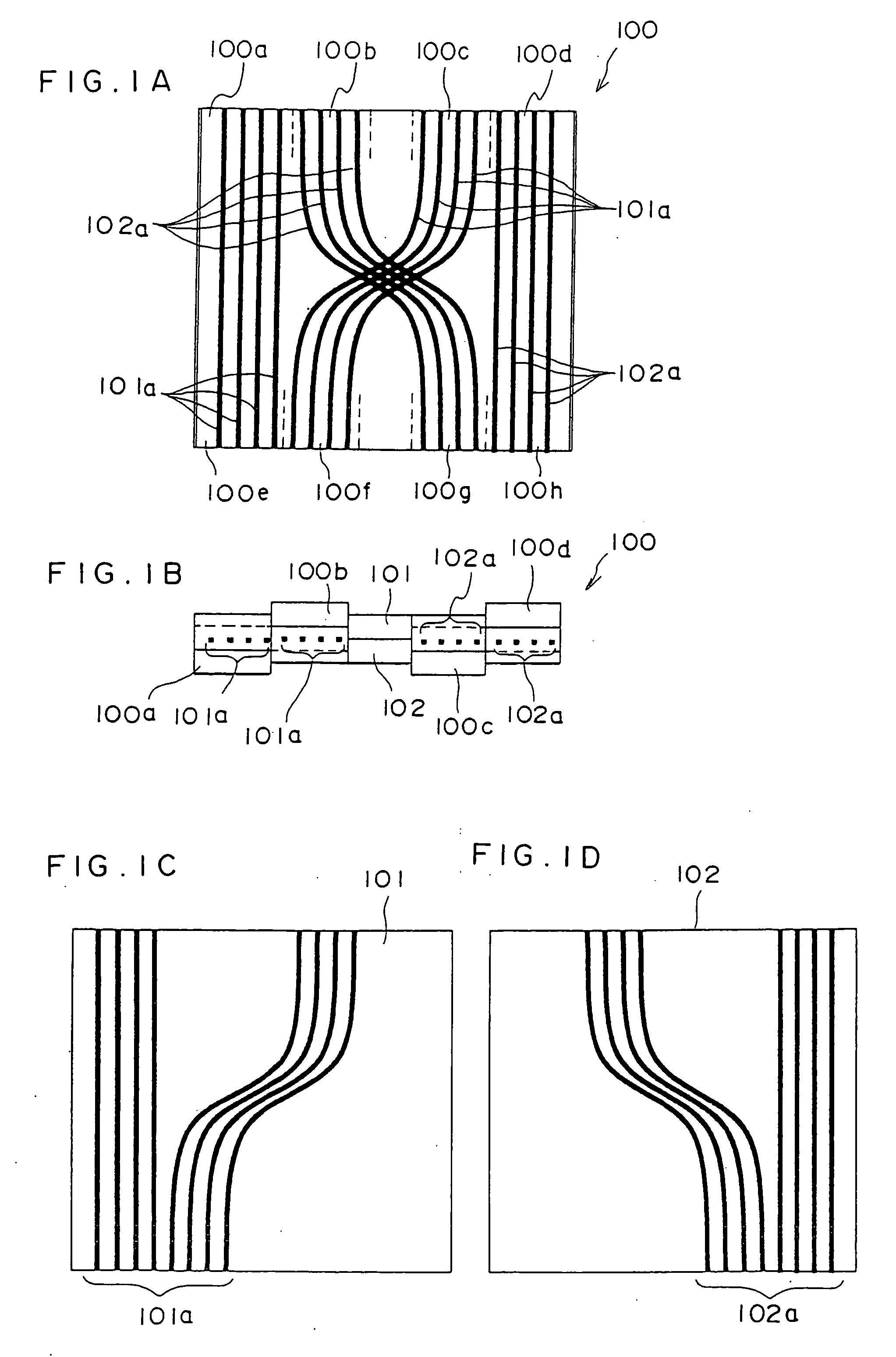
[0144] A thick film resist (SU-8, manufactured by MicroChem Corp.) is applied onto a Si substrate by spin coating, and then the resultant is pre-baked at 80° C., exposed to light through a photomask and developed to form the following: eight convex portions (width: 50 μm, height: 50 μm, length: 50 mm, and adjacent portion pitch: 250 μm), for optical waveguide cores, which each have a square section, as illustrated in FIGS. 1C and 1D; and non-illustrated convex portions (width: 50 μm, height: 50 μm, and length of each side: 2 mm), for alignment marks, which have two square planar sections. Next, this is post-baked at 120° C. to form a master plate for forming optical waveguide cores.

[0145]

[0146] Next, a releasing agent is applied onto this master plate and then a heat-curable dimethylsiloxane resin (SYLGRD 184, manufactured by Dow Corning Asia Ltd.) is poured into this master plate and heated at 120° C. for 30 minutes to be solidified. The resin is then removed as a mold (thic...

example 2

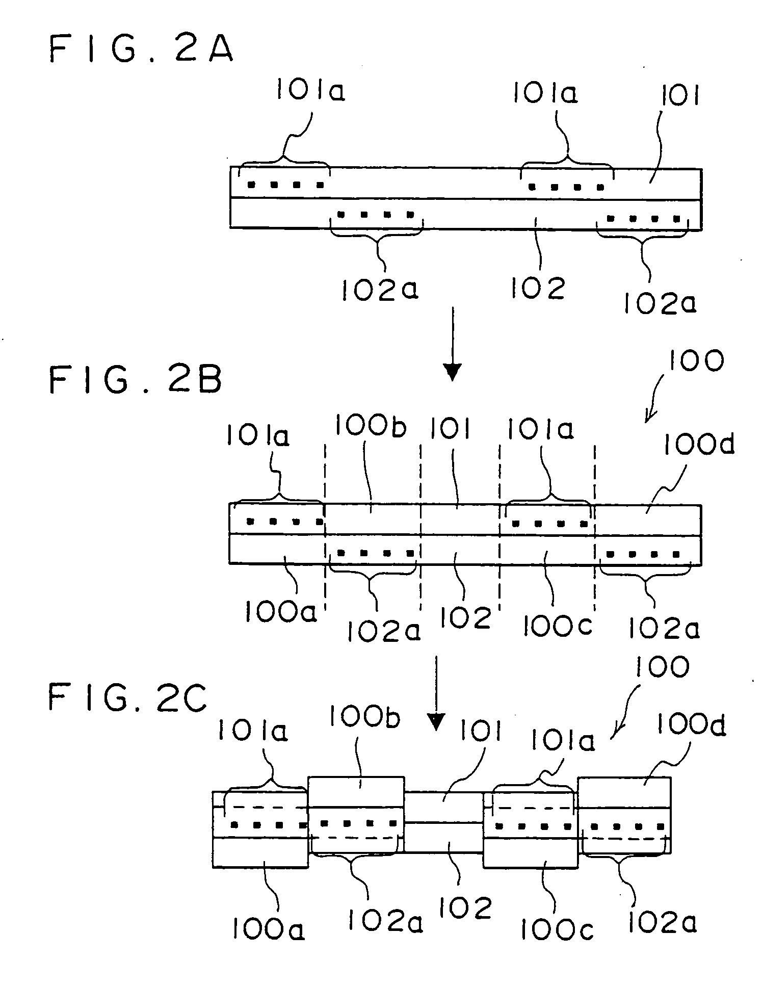
[0154] A master plate and a PDMS mold are first formed in the same way as in Example 1.

[0155]

[0156] The mold and a light-transmissive clad film (Arton film, manufactured by JSR Corp., refractive index: 1.510) of 188 μm design film thickness wherein unnecessary portions are cut off as illustrated in FIGS. 2A and 2B are prepared. The light-transmissive clad film and the mold are brought into close contact with each other. Next, several droplets of an ultraviolet ray-curable resin (PJ3001, manufactured by JSR Corp.) having a viscosity of 1300 mPa·s are dropped into the hole at one end of each of the optical waveguide core concave portions formed in the mold. The air is sucked from the other end at a sucking power of 20 kPa by means of a diaphragm type sucking pump (maximum sucking pressure: 33.25 kPa). As a result, the ultraviolet ray-curable resin is filled into each of the concave portions. Next, UV rays having an energy of 50 mW / cm2 are radiated onto the ultraviolet ray-curable res...


PUM


Abstract

A laminated polymer optical waveguide including two or more optical waveguide films each of which includes an optical waveguide core on a light-transmissive clad film, the two or more optical waveguide films being laminated on each other by using a clad-forming curable resin having a refractive index close to that of the light-transmissive clad film. The laminated polymer optical waveguide includes, at an end thereof, plural strip-shaped structures which each include at least one optical waveguide core and which can be each independently bent in the direction along which the optical waveguide films are laminated.

Description

CROSS-REFERENCE TO RELATED APPLICATION [0001] This application claims priority under 35USC 119 from Japanese Patent Application No. 2003-279743, the disclosure of which is incorporated by reference herein. BACKGROUND OF THE INVENTION [0002] 1. Field of the Invention [0003] The present invention relates to an optical waveguide, in particular, a laminated polymer optical waveguide, and a process for producing the same. [0004] 2. Description of the Related Art [0005] As a method for producing a polymer waveguide, the following methods have been proposed: (1) a method in which a film is impregnated with a monomer, the core part is selectively exposed to light to change the refractive index and the film is then applied (selective polymerization method); (2) a method in which a core layer and a clad layer are applied and then a clad part is formed by using reactive ion etching (RIE method); (3) a method using a photolithographic method in which a ultraviolet ray-curable resin obtained by ...

Claims


Application Information

Patent Timeline
Patent Type & Authority Applications(United States)
IPC IPC(8): G02B6/122G02B6/42G02B6/13
CPCG02B6/1221
Inventor SHIMIZU, KEISHIOHTSU, SHIGEMIYATSUDA, KAZUTOSHIAKUTSU, EIICHI
Owner FUJIFILM BUSINESS INNOVATION CORP
Why Eureka
Try Eureka