Protected organic electronic devices and methods for making the same

a technology of organic electronic devices and protection, which is applied in the direction of organic semiconductor devices, discharge tubes/lamp details, discharge tubes luminescnet screens, etc., can solve the problems of limiting the lifetime of the device, reducing the yield of the product, so as to reduce or eliminate the damage to the display. , the effect of avoiding the display damag

Inactive Publication Date: 2005-02-03
UNIVERSAL DISPLAY
View PDF20 Cites 93 Cited by
  • Summary
  • Abstract
  • Description
  • Claims
  • Application Information

AI Technical Summary

Benefits of technology

[0011] The present invention provides encapsulated OLED device structures, in particular flexible thin film encapsulated structures, that effectively exclude oxygen, moisture, and other harmful species found in the surrounding atmosphere, and at the same time avoid the display damage found to be associated with thin film encapsulation. As disclosed herein, the presence of a conductive polymer layer in direct contact with the organic small-molecule region of an OLED device structure that has been provided with a thin film encapsulation region significantly increases product yield by minimizing or eliminating the display damage seen in device structures provided with a thin encapsulation region in the absence of the present invention conductive polymer layer.

Problems solved by technology

Low work function metals, however, are chemically reactive; exposure to and subsequent reaction with oxygen and moisture can severely limit the lifetime of the devices.
Moisture and oxygen are also known to produce other deleterious effects, for instance, reactions with the organic materials themselves.
However, it has been observed that display damage, for instance, in the form of pixel shorting, bubbling or delamination, often attends the formation of such encapsulated OLED device structures.

Method used


Image

  • Protected organic electronic devices and methods for making the same
  • Protected organic electronic devices and methods for making the same
  • Protected organic electronic devices and methods for making the same

Examples


example 1

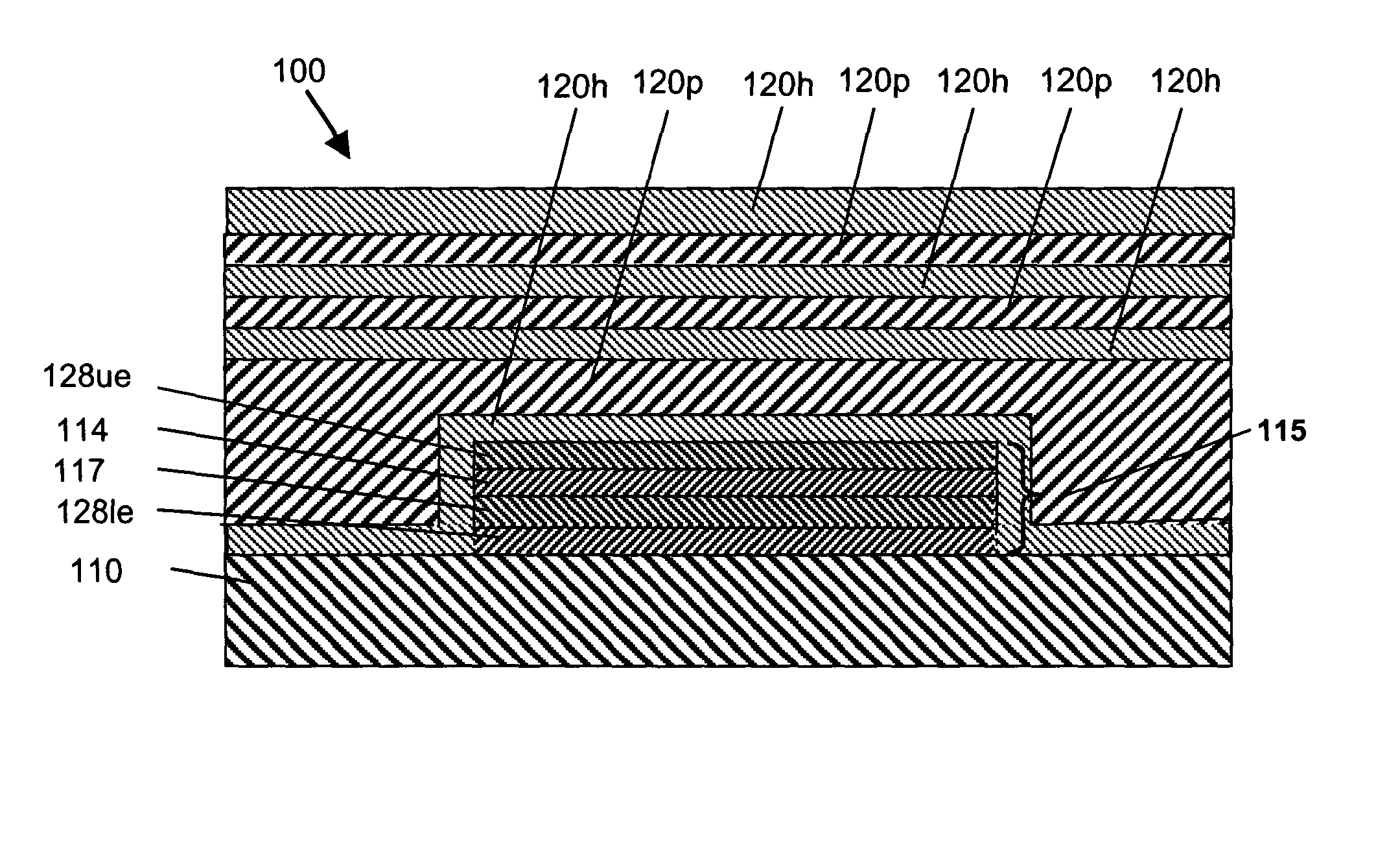
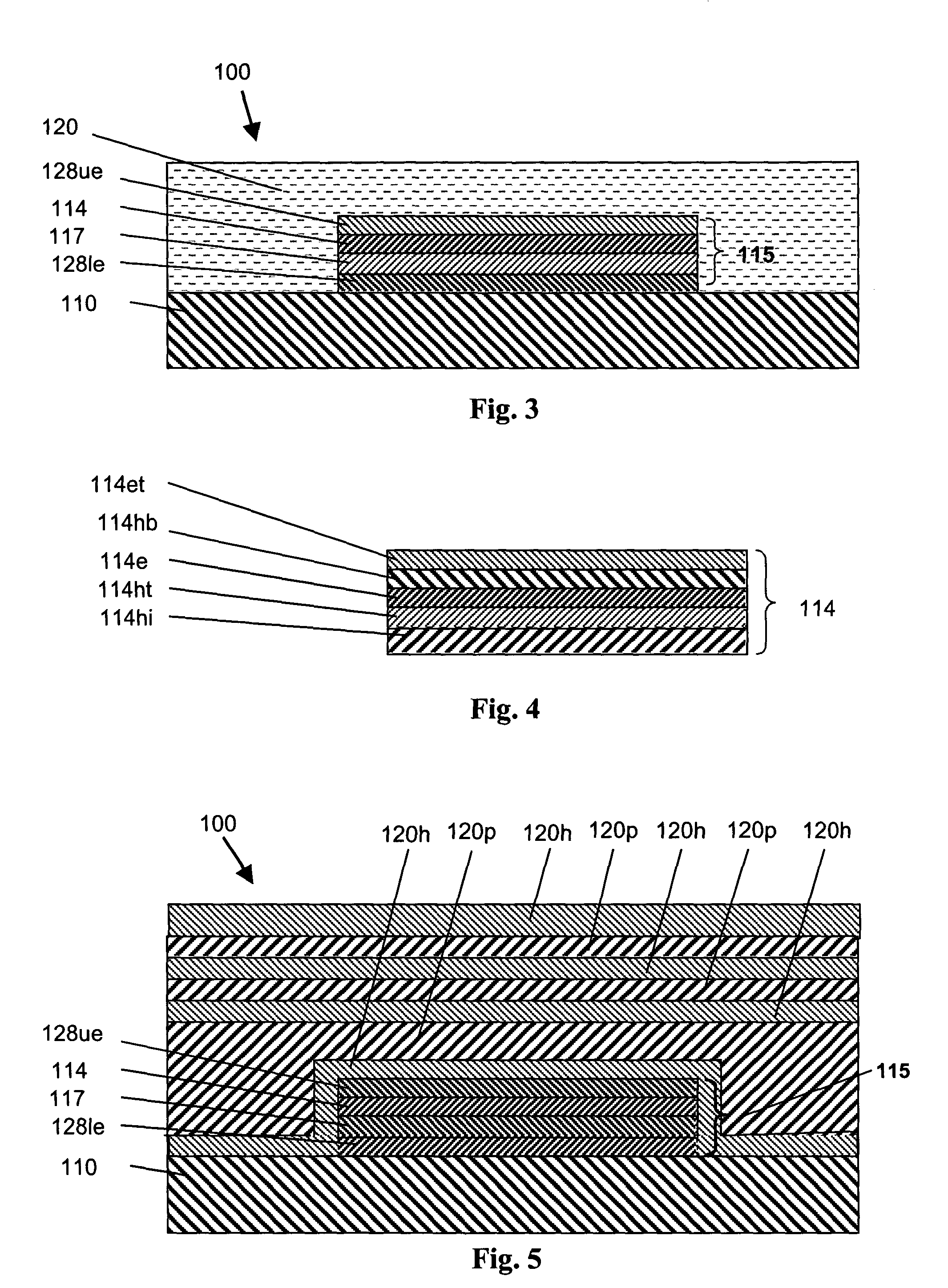
[0051] The following describes a process in accordance with the present invention for the formation of a thin film encapsulated OLED display, specifically a flexible OLED which process will now be described with reference to FIG. 7.

[0052] The substrate 110 in this example is a flexible substrate consisting of substrate layer 110s and a multilayer barrier stack 110 ml (layers not separately illustrated). The substrate layer 110s in this example is barrier coated polyethylene terephthalate (PET) of thickness 7 mil (178 μm). The multilayer barrier stack 110 ml consists of alternating layers of an organic polymer (i.e., polyacrylate) as a planarizing material and an inorganic dielectric (i.e., aluminum oxide, Al2O3) as a high-density material. There are approximately 5 alternating pairs of these materials on the substrate. The first polymer layer planarizes the surface to make it smooth, while subsequent polymer layers serve to decouple any defects in the inorganic dielectric. The inor...

example 2

[0058] Encapsulated displays were made in accordance with the process described in Example 1, either with or without a PEDOT-PSS layer. All devices were examined and tested approximately one week after manufacture. In the devices without the PEDOT-PSS polymeric layer, pixels were observed to fail within the first few minutes of display illumination, resulting in blisters / delamination. In analogous devices containing the PEDOT-PSS polymeric layer, on the other hand, blisters / delamination were not observed, and such pixel failure was minimal or non-existent. Indeed, pixels in devices containing the polymeric layer of the invention were observed to continue functioning after 100 hours or more of illumination.

[0059] The results show that by providing an intervening conductive polymer layer as disclosed herein (e.g., a PEDOT-PSS layer), between the anode and the overlying organic small-molecule layer in a device having a thin film encapsulation region, display damage associated with the...


PUM


Abstract

An organic light emitting device structure is provided, which comprises: (a) a substrate; (b) a first electrode disposed over the substrate; (c) a polymeric layer comprising a conductive polymer disposed over the first electrode; (d) an organic layer consisting essentially of small molecule material disposed over and in direct contact with said polymeric layer; (e) a second electrode disposed over the organic layer; and (f) a thin film encapsulation region disposed over the second electrode. An organic light emitting device is also provided, which comprises: (a) a polymer layer comprising a hole injecting conductive polymer and (b) a small molecule layer comprising an emissive small molecule material. In certain embodiments, the small molecule layer further comprises a small molecule hole injection layer.

Description

FIELD OF THE INVENTION [0001] The present invention relates to organic light emitting diode devices which are protected from environmental elements such as moisture and oxygen and which display enhanced durability and reliability. BACKGROUND OF THE INVENTION [0002] Organic light emitting diodes (OLEDs) are becoming increasingly important from an economic standpoint. For example, OLEDs are potential candidates for a wide variety of virtual- and direct-view type displays, such as lap-top computers, televisions, digital watches, telephones, pagers, cellular telephones, calculators and the like. Unlike inorganic semiconductor light emitting devices, organic light emitting devices are generally simple and are relatively easy and inexpensive to fabricate. Also, OLEDs readily lend themselves to applications requiring a wide variety of colors and to applications that concern large-area devices. [0003] In general, two-dimensional OLED arrays for imaging applications are known in the art, and...

Claims


Application Information

Patent Timeline
Patent Type & Authority Applications(United States)
IPC IPC(8): H01J1/62H01LH01L51/52
CPCH01L2251/5338H01L51/5237H10K50/846H10K50/844H10K2102/311
Inventor CHWANG, ANNAHACK, MICHAEL
Owner UNIVERSAL DISPLAY
Why Eureka
Try Eureka