

Optical module and manufacturing method of the same, optical-communication apparatus, and electronic apparatus
a technology of optical modules and manufacturing methods, applied in multiplex communication, instruments, optical elements, etc., can solve the problems of difficult securing of mechanical strength, difficult securing of a position of optical elements and optical fibers, and bending of substrates, so as to achieve simplification of manufacturing process, reduce transmission loss in high frequency region, and simplify the structure
- Summary
- Abstract
- Description
- Claims
- Application Information
AI Technical Summary
Benefits of technology
Problems solved by technology
Method used
Image

Examples
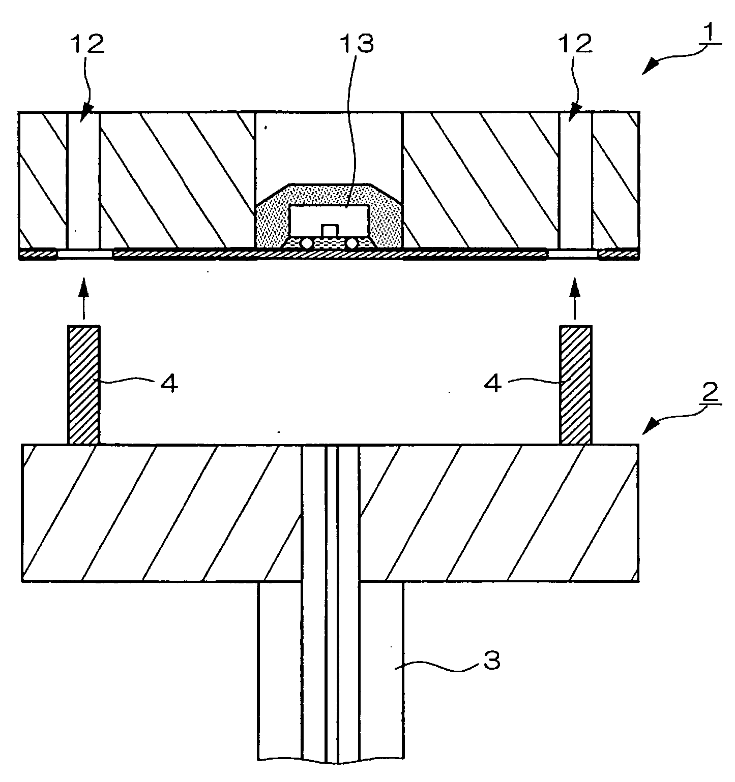
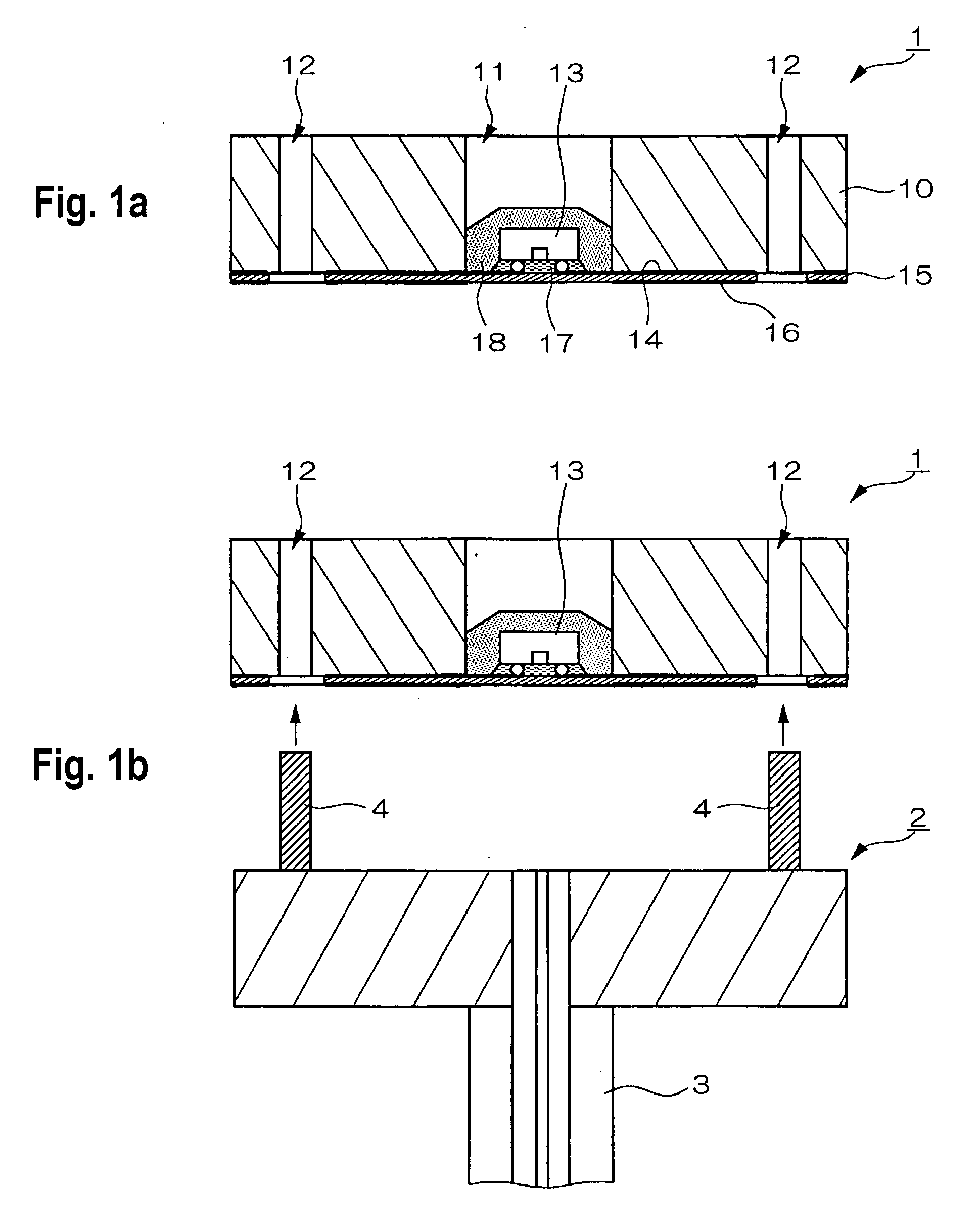
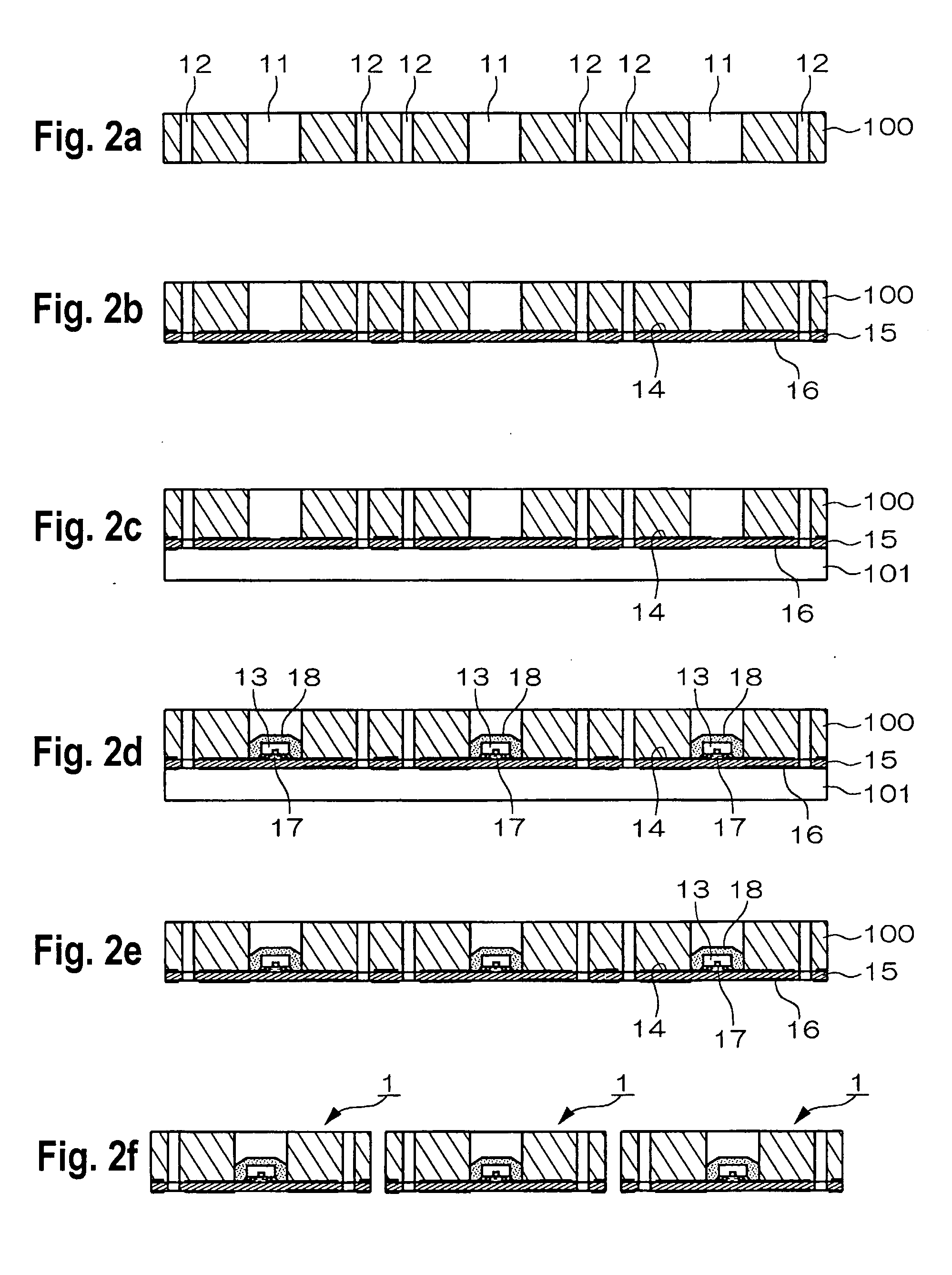
first embodiment
[0068] In the above-described first embodiment, the optical module, which does not include a drive circuit or the like for driving the optical element 13, has been described as an example, however, the optical module can be constituted including these.
[0069]FIG. 3 is a view explaining a structure of an optical module according to a second embodiment. The basic structure of the optical module 1a shown in this view is the same as that of the optical module 1 according to the above-described first embodiment, and further includes a circuit chip 20, which constitutes an electric circuit together with the optical element 13. Specifically, as for the circuit chip 20, a driver, which drives the light emitting element, or an amplifier, which amplifies the output current of the light receiving element, or the like can be cited. In addition, although the illustration is omitted, the optical module 1a may be constituted including passive elements such as a resistor and a capacitor, and various...
third embodiment
[0076]FIG. 4 is a view explaining a structure of an optical module according to a An optical module 1b according to the embodiment is not the one that is detachable to the connector supporting the optical fiber described in each of the above embodiments, but the one that is used as being mounted on a circuit board 5 (an opto / electric mixed substrate) including an optical waveguide 6, as illustrated.
second embodiment
[0077] The optical module 1b shown in this view is basically provided with the same structure as the optical module 1a according to the above-described second embodiment, however, the optical module 1b differs, in that the second hole used for the alignment of the connector is omitted and that an optical waveguide 24 is added. The same numerals are given to the common components, and thus the description thereof will be omitted.
[0078] The optical waveguide 24 is coupled to the optical waveguide 6 provided on the circuit board 5, and has a function to transmit the light signal radiated from the optical element 13 or the light signal sent form the outside. At the coupling point of the optical waveguide 24 and the optical waveguide 6 on the circuit board 5 side, a matching oil or the like, which properly reduces optical loss, is used. The optical module 24 is arranged such that the extension direction thereof is substantially in parallel with one surface side of a substrate 10a. Then, ...
PUM
 Abstract
Description
Claims
Application Information