Semiconductor device and method for fabricating the same

a technology of semiconductor devices and ohmic contact electrodes, which is applied in the direction of semiconductor devices, semiconductor/solid-state device details, electrical apparatus, etc., can solve the problems of high annealing temperature and complicated manufacturing procedures, poor ohmic contact electrode surface after annealing process, and insufficient for subsequent metal wire bonding, etc., to achieve stable power output

Inactive Publication Date: 2005-02-10
INST NUCLEAR ENERGY RES ROCAEC
View PDF3 Cites 16 Cited by
  • Summary
  • Abstract
  • Description
  • Claims
  • Application Information

AI Technical Summary

Benefits of technology

[0016] The objective of the present invention is to provide a light-emitting device and method for fabricating the same, which uses a new P-type ohmic contact electrode to have a stable power output.
[0019] Compared with the prior art, the present invention possesses following advantages:
[0021] 2. The P-type ohmic contact electrode still possesses a uniform surface morphology after the annealing process is performed, and the metal wire can be bonded on the surface of the P-type ohmic contact electrode directly without an extra gold layer for the wire bonding. As a result, the present invention only needs one mask for defining the position and the size of the P-type ohmic contact electrode, thus the present invention can simplify the fabrication process.
[0022] 3. The present light-emitting device has a wider linear range in the input current / output power curve. Furthermore, under the same input current, the present light-emitting device has higher output power.

Problems solved by technology

However, the currently available light-emitting devices require a higher annealing temperature and a more complicated manufacturing procedure to form an electrode with a good ohmic contact property.
), and the surface of the ohmic contact electrode after the annealing process is very rough and inadequate for the subsequent metal wire bonding.
Additionally, at least two lithographic processes are required, so the manufacturing procedure is complicated.
However, the annealing process at the high temperature between 380° C. and 400° C. will result in deterioration of the surface of the P-type ohmic contact electrode 30, which is inadequate for the subsequent metal wire bonding.
Obviously, the surface of P-type ohmic contact electrode 30 has many concaves and convexes, which is inadequate for the subsequent metal wire bonding.
From the above-mentioned prior art, the formation of the P-type ohmic contact electrode requires a higher annealing temperature, which will result in the unwanted cross-diffusion between layers of the epitaxial structure and damage the optoelectrical property ofthe device.

Method used


Image

  • Semiconductor device and method for fabricating the same
  • Semiconductor device and method for fabricating the same
  • Semiconductor device and method for fabricating the same

Examples


first embodiment

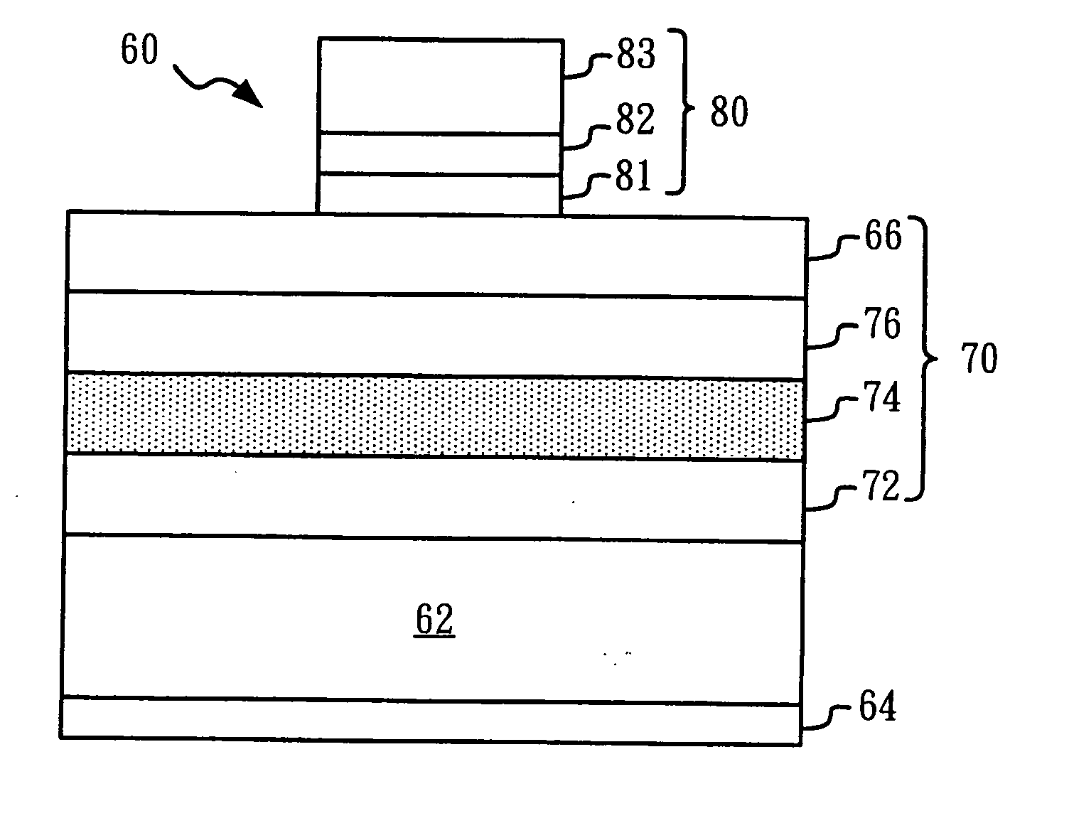
[0037]FIG. 6 is a cross-sectional diagram of a light-emitting device 60 according to the present invention. As shown in FIG. 6, the light-emitting device 60 comprises an N-type GaAs substrate 62, an epitaxial structure 70 positioned on the upper surface of the N-type GaAs substrate 62, an N-type ohmic contact electrode 64 positioned on the bottom surface of the N-type GaAS substrate 62, and a P-type ohmic contact electrode 80 positioned on the epitaxial structure 70. The epitaxial structure 70 consists of a first reflection layer 72, a light-emitting layer 74, a second reflection layer 76 and a P-type GaAs contact layer 66. The carrier density of the P-type GaAs contact layer 66 is more than 1019 / cm3, and the reflectivity of the first reflection layer 72 is more than or equal to that of the second reflection layer 76.

[0038] The P-type ohmic contact electrode 80 of the present invention can be a three-layer structure including a first nickel layer 81 positioned on the P-type GaAs con...

second embodiment

[0044]FIG. 11 is a cross-sectional diagram of a light-emitting device 90 according to the present invention. As shown in FIG. 11, the P-type ohmic contact electrode 80 of the light-emitting device 90 is a five-layer structure. The P-type ohmic contact electrode 80 of the light-emitting device 90 further comprises a nickel-chrome alloy layer 84 and a second gold layer 85 in addition to the first nickel layer 81, the first platinum layer 82 and the first gold layer 83. A pure nickel layer or a pure chrome layer also can replace the nickel-chrome alloy layer 84, and the metal wire is bonded on the surface of the second gold layer 85 directly.

third embodiment

[0045]FIG. 12 is a cross-sectional diagram of a light-emitting device 100 according to the present invention. As shown in FIG. 12, the P-type ohmic contact electrode 80 of the light-emitting device 100 is a six-layer structure. The P-type ohmic contact electrode 80 of the light-emitting device 100 further comprises a metal layer 86, a second platinum layer 87 and a third gold layer 88 in addition to the first nickel layer 81, the first platinum layer 82 and the first gold layer 83. The metal layer 86 also can be made of nickel or titanium, and the metal wire is bonded on the surface of the third gold layer 88 directly.

[0046] Compared with the prior art, the present light-emitting de possesses the following advantages:

[0047] 1. The annealing temperature for forming the P-type ohmic contact electrode and the N-type ohmic contact electrode can be reduced to a range between 220 and 330° C., which can avoid to damage the device by dramatically reducing the cross-diffusion between the la...


PUM

PropertyMeasurementUnit
thicknessaaaaaaaaaa
thicknessaaaaaaaaaa
temperatureaaaaaaaaaa

Abstract

A light-emitting device and method for fabricating the same are revealed. The light-emitting device includes an epitaxial structure, a P-type ohmic contact electrode and an N-type ohmic contact electrode. The epitaxial structure includes a plurality of epitaxial layers capable of emitting light and P-type contact layer. The P-type ohmic contact electrode includes a first nickel layer deposited on the epitaxial structure, a first platinum layer deposited on the first nickel layer, and a first gold layer deposited on the first platinum layer. According to the fabricating method of the light-emitting device, an epitaxial structure is first formed on the surface of a substrate, a P-type ohmic contact electrode is then formed on the epitaxial structure, and an N-type ohmic contact electrode is formed on the other surface of the substrate. Finally, an annealing process is performed at a temperature between 220° C. and 330° C.

Description

RELATED U.S. APPLICATIONS [0001] Not applicable. STATEMENT REGARDING FEDERALLY SPONSORED RESEARCH OR DEVELOPMENT [0002] Not applicable. REFERENCE TO MICROFICHE APPENDIX [0003] Not applicable. FIELD OF THE INVENTION [0004] The present invention relates to a semiconductor device and method for fabricating the same, and more particularly, to a light-emitting device and method for fabricating the same, which has a stable output power due to using a new P-type ohmic contact electrode. BACKGROUND OF THE INVENTION [0005] The ohmic contact electrode provides an important medium and path for the operational current required by the light-emitting device. However, the currently available light-emitting devices require a higher annealing temperature and a more complicated manufacturing procedure to form an electrode with a good ohmic contact property. Therefore, how to improve the property of the ohmic contact electrode and simplify the manufacturing procedure to reduce the cost becomes the imp...

Claims


Application Information

Patent Timeline
Patent Type & Authority Applications(United States)
IPC IPC(8): H01L27/15H01L29/45H01L33/30H01L33/40
CPCH01L33/40H01L33/30
Inventor WU, CHIH-HUNG
Owner INST NUCLEAR ENERGY RES ROCAEC
Why Eureka
Try Eureka