Schottky barrier diode and manufacturing method thereof

a technology of schottky barrier and manufacturing method, which is applied in the direction of diodes, semiconductor devices, electrical apparatus, etc., can solve problems such as reducing resistance, and achieve the effect of small capacitance and low forward voltage v

Inactive Publication Date: 2005-02-10
COLLABO INNOVATIONS INC
View PDF1 Cites 15 Cited by
  • Summary
  • Abstract
  • Description
  • Claims
  • Application Information

AI Technical Summary

Benefits of technology

[0011] The object of the present invention is to provide a Schottky barrier diode which achieves a lower forward voltage Vf and a smaller capacitance than the above-mentioned conventional Schottky barrier diode, without an increase in a reverse leakage current, and a manufacturing method for the same.

Problems solved by technology

Thus, the area of the buried layer is smaller than in the above-mentioned conventional Schottky barrier diode, thereby reducing a resistance.

Method used


Image

  • Schottky barrier diode and manufacturing method thereof
  • Schottky barrier diode and manufacturing method thereof
  • Schottky barrier diode and manufacturing method thereof

Examples


Embodiment Construction

[0049] The following part describes an embodiment of the present invention with reference to the attached figures.

[0050] It should be noted that the same reference numerals are used to indicate the same constituents in any of the figures.

[0051] (Construction)

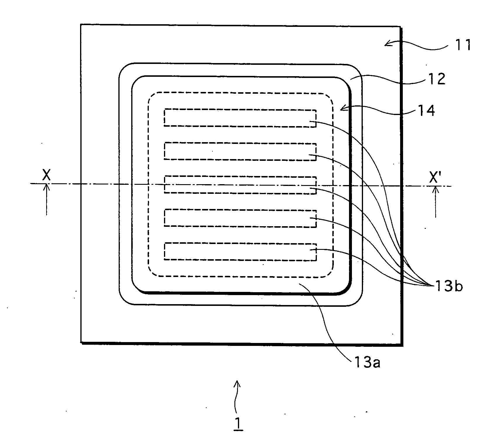
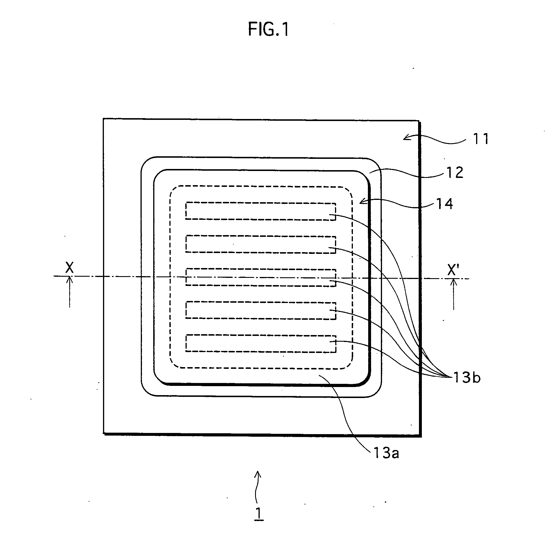
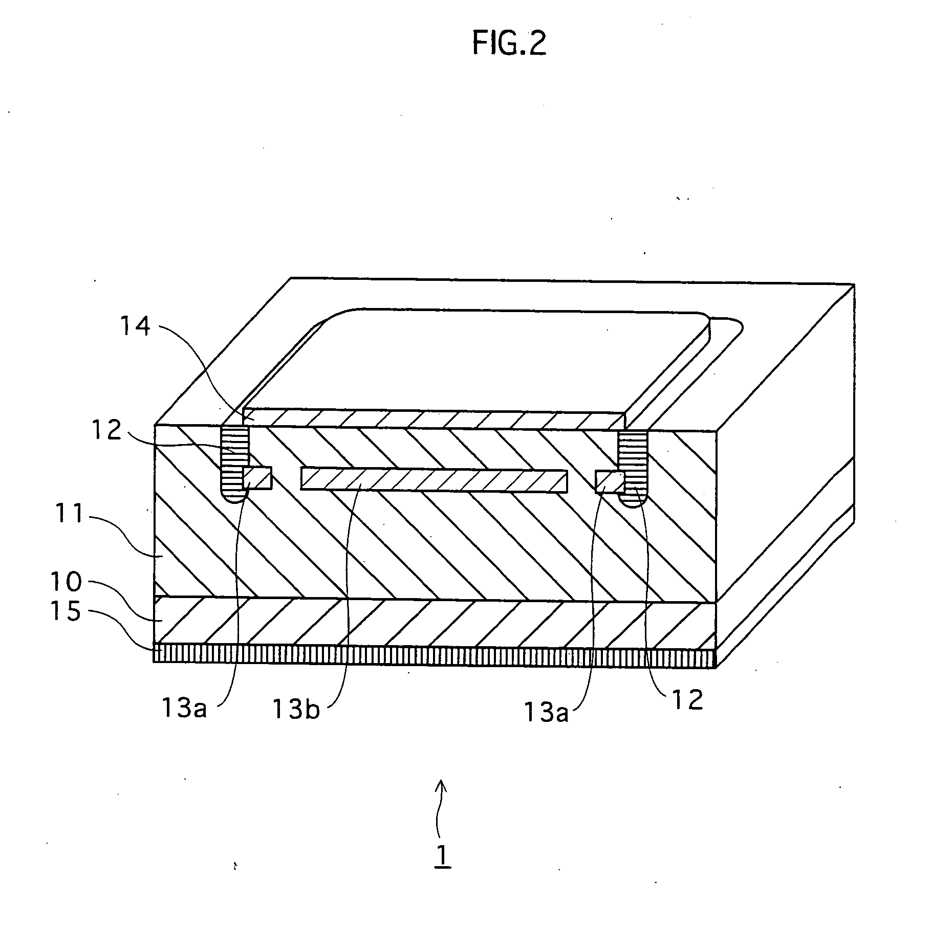
[0052]FIG. 1 is a plan view illustrating a Schottky barrier diode relating to an embodiment of the present invention, as viewed from an anode-electrode side. FIG. 2 is a perspective view illustrating a vertical cross section, along a line X-X′ shown in FIG. 1, of the Schottky barrier diode.

[0053] A Schottky barrier diode 1 shown in FIGS. 1 and 2 is constituted by a cathode electrode 15, an n+ substrate 10, an n epitaxial layer 11, a guard ring 12, a buried layer 13a, a buried layer 13b, and an anode electrode 14.

[0054] The n+ substrate 10 is made of n-type silicon (Si) having a high concentration of donor impurities. The n epitaxial layer 11 is made of n-type Si with a low concentration of donor impurities, which is precipi...


PUM


Abstract

To reduce a reverse leakage current in a Schottky barrier diode with achieving a lower forward voltage Vf and a smaller capacitance than in the related art, a Schottky barrier diode includes a semiconductor layer of a first conductivity type, a first electrode which is a metal layer forming a Schottky contact with a main surface of the semiconductor layer, a second electrode forming an ohmic contact with an opposite main surface of the semiconductor layer, a buried layer of a second conductivity type formed within the semiconductor layer so as not to be in contact with the first electrode, where the second conductivity type has a different charge carrier from the first conductivity type, and a guard ring of the second conductivity type formed within the semiconductor layer so as to be in contact with the first electrode and also to surround the buried layer without contacting with the buried layer.

Description

BACKGROUND OF THE INVENTION [0001] (1) Field of the Invention [0002] The present invention relates to a Schottky barrier diode. The present invention especially relates to a low-loss Schottky barrier diode which achieves a lower forward voltage Vf and a smaller capacitance, without an increase in a reverse leakage current. [0003] (2) Prior Art [0004] In recent years, Schottky barrier diodes are widely used as rectifying elements in electronic products in order to achieve lower power consumption and higher speed. Schottky barrier diodes have a lower forward voltage Vf and a smaller capacitance than general pn-junction diodes. [0005] A forward voltage Vf of a Schottky barrier diode decreases as a barrier height is lowered. However, a decrease in Schottky barrier height causes a problem that reverse currents that are generated when a reverse bias is applied, i.e. a leakage current, increase. [0006] To solve this problem, unexamined Japanese patent application publication No. H11-330498...

Claims


Application Information

Patent Timeline
Patent Type & Authority Applications(United States)
IPC IPC(8): H01L21/329H01L27/08H01L29/06H01L29/872
CPCH01L27/0814H01L29/872H01L29/66143H01L29/0692
Inventor TANAKA, YUJIKASHIMA, NAOTOSHI
Owner COLLABO INNOVATIONS INC
Why Eureka
Try Eureka