Phased array antenna with edge elements and associated methods

a phased array and edge element technology, applied in the field of communication, can solve the problems of limiting the bandwidth and directivity capabilities of such antennas, affecting the performance of the array of dipole antenna elements, and affecting the performance of the array, so as to increase the capacitive coupling therebetween, and increase the capacitive coupling

Inactive Publication Date: 2005-02-10
HARRIS CORP
View PDF13 Cites 15 Cited by
  • Summary
  • Abstract
  • Description
  • Claims
  • Application Information

AI Technical Summary

Benefits of technology

[0020] To further increase the capacitive coupling between adjacent legs of adjacent dipole antenna elements, a respective impedance element may be electrically connected between the spaced apart end portions of adjacent legs of adjacent dipole antenna elements. In other embodiments, a respective printed impedance element may be positioned adjacent the spaced apart end portions of adjacent legs of adjacent dipole antenna elements for further increasing the increased capacitive coupling therebetween.
[0021] Another aspect of the present invention is directed to a method of making a phased array antenna on a substrate having a first surface, and a second surface adjacent thereto and defining an edge therebetween. The method comprises forming a plurality of dipole antenna elements on the first surface and at least a portion of at least one dipole antenna element on the second surface. Each dipole antenna element may comprise a medial feed portion and a pair of legs extending outwardly therefrom, and adjacent legs of adjacent dipole antenna elements on the first and second surfaces include respective spaced apart end portions having predetermined shapes and relative positioning for providing increased capacitive coupling between the adjacent dipole antenna elements.

Problems solved by technology

The bandwidth and directivity capabilities of such antennas, however, can be limiting for certain applications.
However, utilizing an array of dipole antenna elements presents a dilemma.
The maximum grating lobe free scan angle can be increased if the dipole antenna elements are spaced closer together, but a closer spacing can increase undesirable coupling between the elements, thereby degrading performance.
This undesirable coupling changes rapidly as the frequency varies, making it difficult to maintain a wide bandwidth.
However, design constraints for certain applications may limit the array size so that it has a significantly reduced number of active dipole antenna elements.
However, the additional feed lines for the dummy dipole antenna elements increase the complexity of the phased array antenna.

Method used


Image

  • Phased array antenna with edge elements and associated methods
  • Phased array antenna with edge elements and associated methods
  • Phased array antenna with edge elements and associated methods

Examples


Embodiment Construction

[0035] The present invention will now be described more fully hereinafter with reference to the accompanying drawings, in which preferred embodiments of the invention are shown. This invention may, however, be embodied in many different forms and should not be construed as limited to the embodiments set forth herein. Rather, these embodiments are provided so that this disclosure will be thorough and complete, and will fully convey the scope of the invention to those skilled in the art. Like numbers refer to like elements throughout, and prime, double prime and triple prime notations are used to indicate similar elements in alternate embodiments.

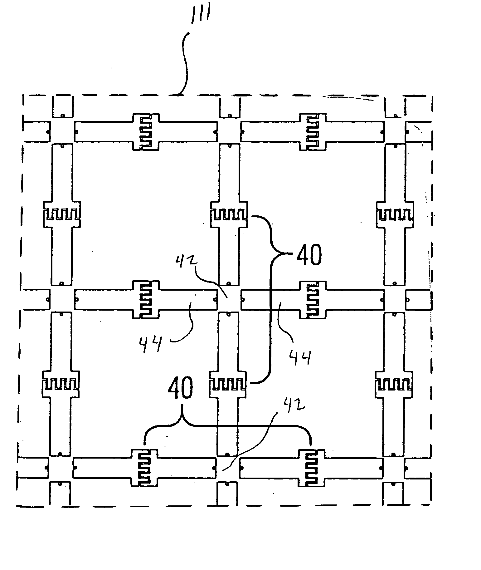
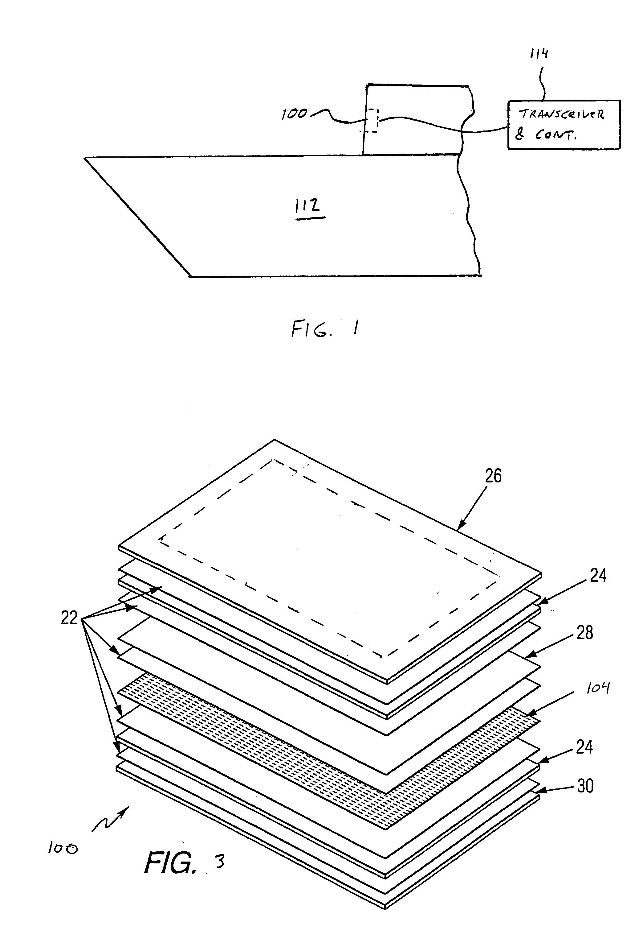
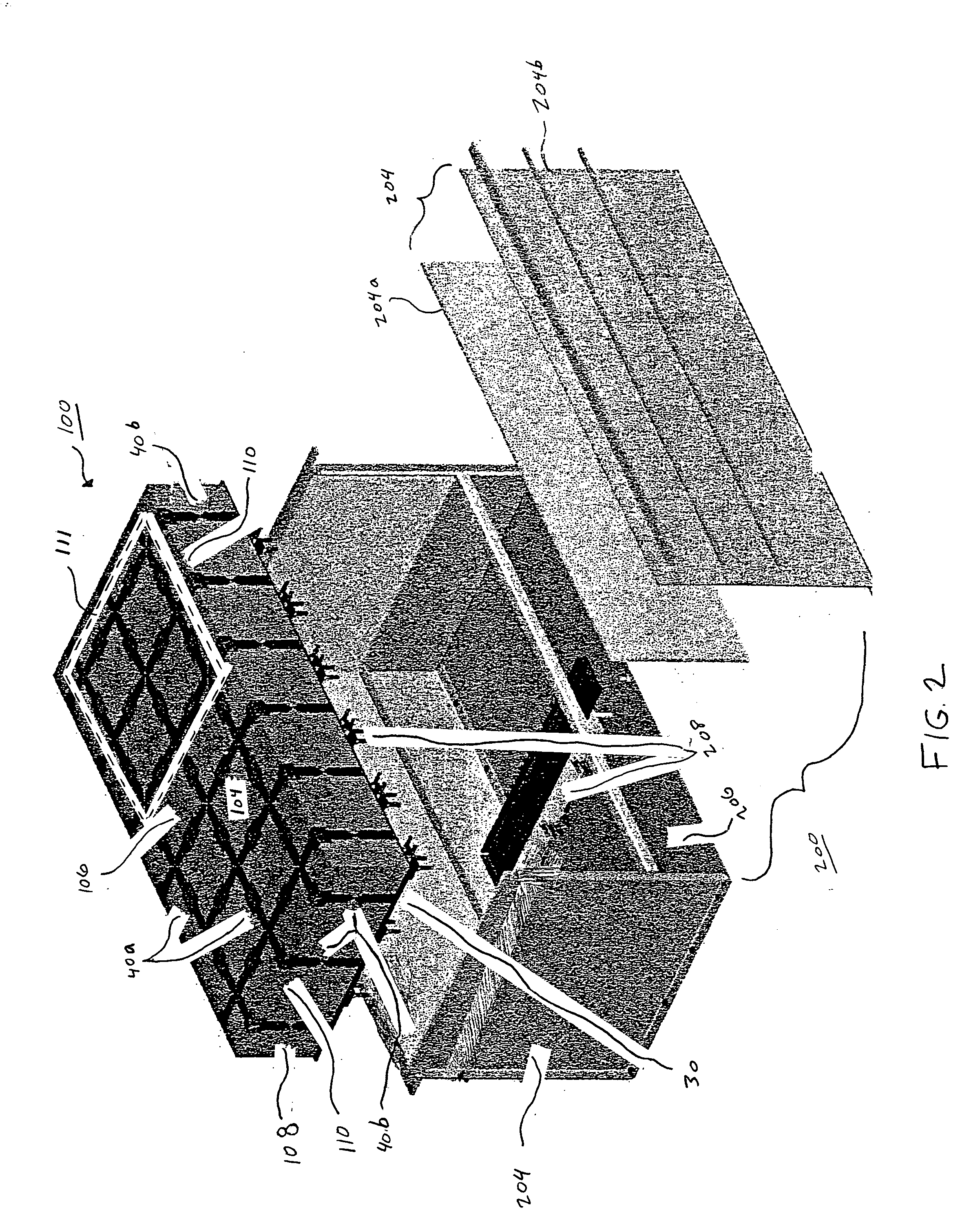
[0036] Referring initially to FIGS. 1 and 2, a wideband phased array antenna 100 in accordance with the present invention will now be described. The phased array antenna 100 is particularly advantageous when design constraints limit the number of active dipole antenna elements in the array. The design constraints may be driven by a platform ...


PUM


Abstract

A phased array antenna includes a substrate having a first surface, and a second surface adjacent thereto and defining an edge therebetween. A plurality of dipole antenna elements are on the first surface, and at least a portion of at least one dipole antenna element is on the second surface. Each dipole antenna element includes a medial feed portion and a pair of legs extending outwardly therefrom. Adjacent legs of adjacent dipole antenna elements on the first and second surfaces include respective spaced apart end portions having predetermined shapes and relative positioning for providing increased capacitive coupling between the adjacent dipole antenna elements.

Description

FIELD OF THE INVENTION [0001] The present invention relates to the field of communications, and more particularly, to phased array antennas. BACKGROUND OF THE INVENTION [0002] Existing microwave antennas include a wide variety of configurations for various applications, such as satellite reception, remote broadcasting, or military communication. The desirable characteristics of low cost, light weight, low profile and mass producibility are provided in general by printed circuit antennas. The simplest forms of printed circuit antennas are microstrip antennas wherein flat conductive elements, such as monopole or dipole antenna elements, are spaced from a single essentially continuous ground plane by a dielectric sheet of uniform thickness. An example of a microstrip antenna is disclosed in U.S. Pat. No. 3,995,277 to Olyphant. [0003] The antennas are designed in an array and may be used for communication systems such as identification of friend / foe (IFF) systems, personal communication...

Claims


Application Information

Patent Timeline
Patent Type & Authority Applications(United States)
IPC IPC(8): H01Q9/16H01Q9/28H01Q21/06
CPCH01Q9/16H01Q21/062H01Q9/28H01Q1/38H01Q3/46H01Q9/045H01Q9/065H01Q17/007
Inventor CROSWELL, WILLIAM F.TAYLOR, ROBERT C.JONES, ANTHONY M.DURHAM, TIMOTHY E.
Owner HARRIS CORP
Why Eureka
Try Eureka