Structure and method for fine pitch flip chip substrate

a technology of flip chip and substrate, which is applied in the direction of printing circuit manufacturing, printed circuit aspects, and metal adhesion improvement of the insulation substrate, etc., can solve the problems of poor adhesion of metal wires to the underfill and reduce reliability

Inactive Publication Date: 2005-02-10
KINSUS INTERCONNECT TECH
View PDF7 Cites 10 Cited by
  • Summary
  • Abstract
  • Description
  • Claims
  • Application Information

AI Technical Summary

Benefits of technology

[0007] The present invention provides a Fine Pitch flip chip substrate structure, as shown in FIG. 1B. A black oxide dam is formed on the metal wires between the bump pads to replace the conventional solder resist. The thickness of the dam can be easily controlled between 1-

Problems solved by technology

The inherent shortcoming of this method is that the metal wires are not well adherent to the underfil

Method used


Image

  • Structure and method for fine pitch flip chip substrate
  • Structure and method for fine pitch flip chip substrate
  • Structure and method for fine pitch flip chip substrate

Examples


Embodiment Construction

[0034]FIGS. 2A to 2T show the steps of the method for making a flip chip substrate and includes the following steps:

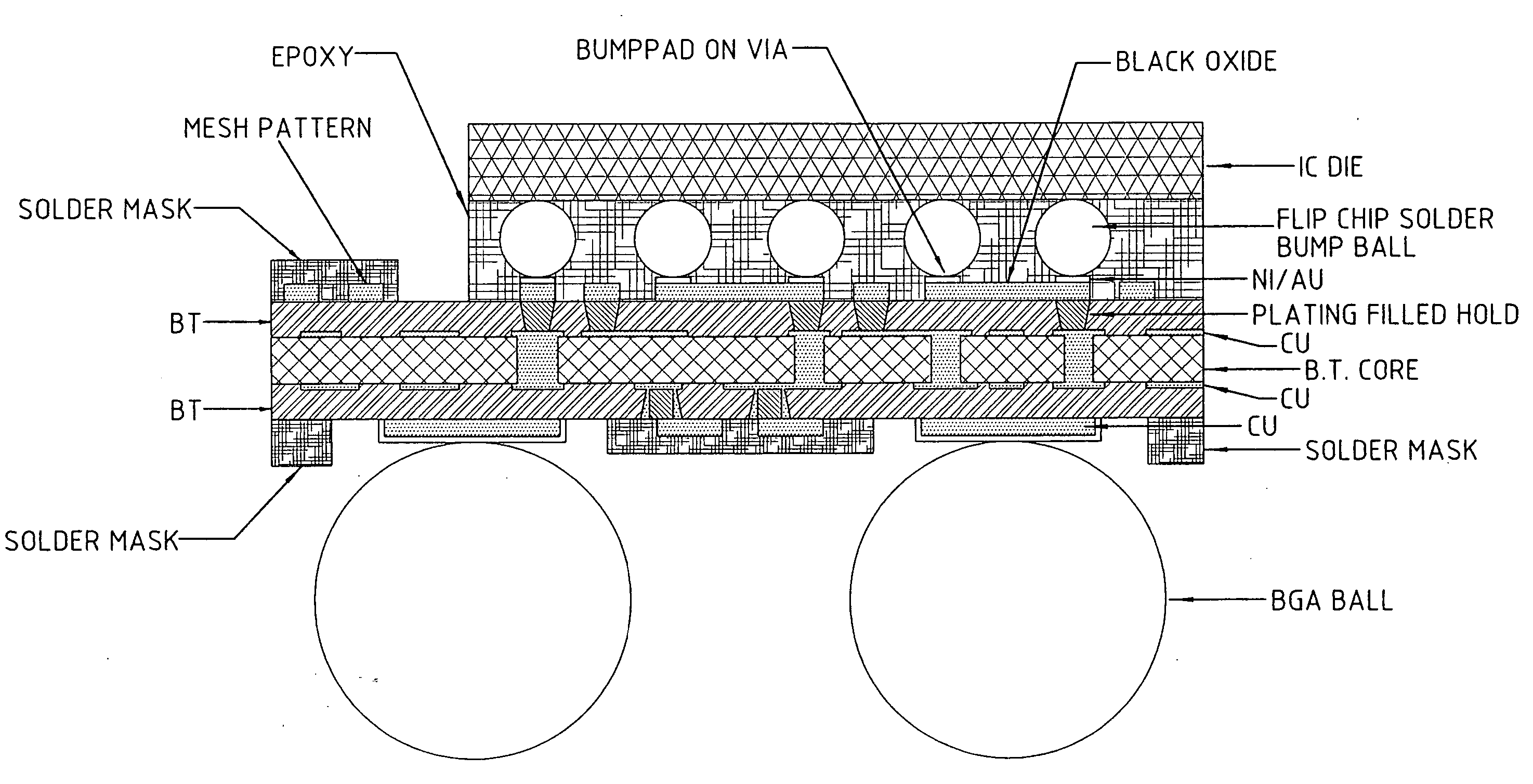
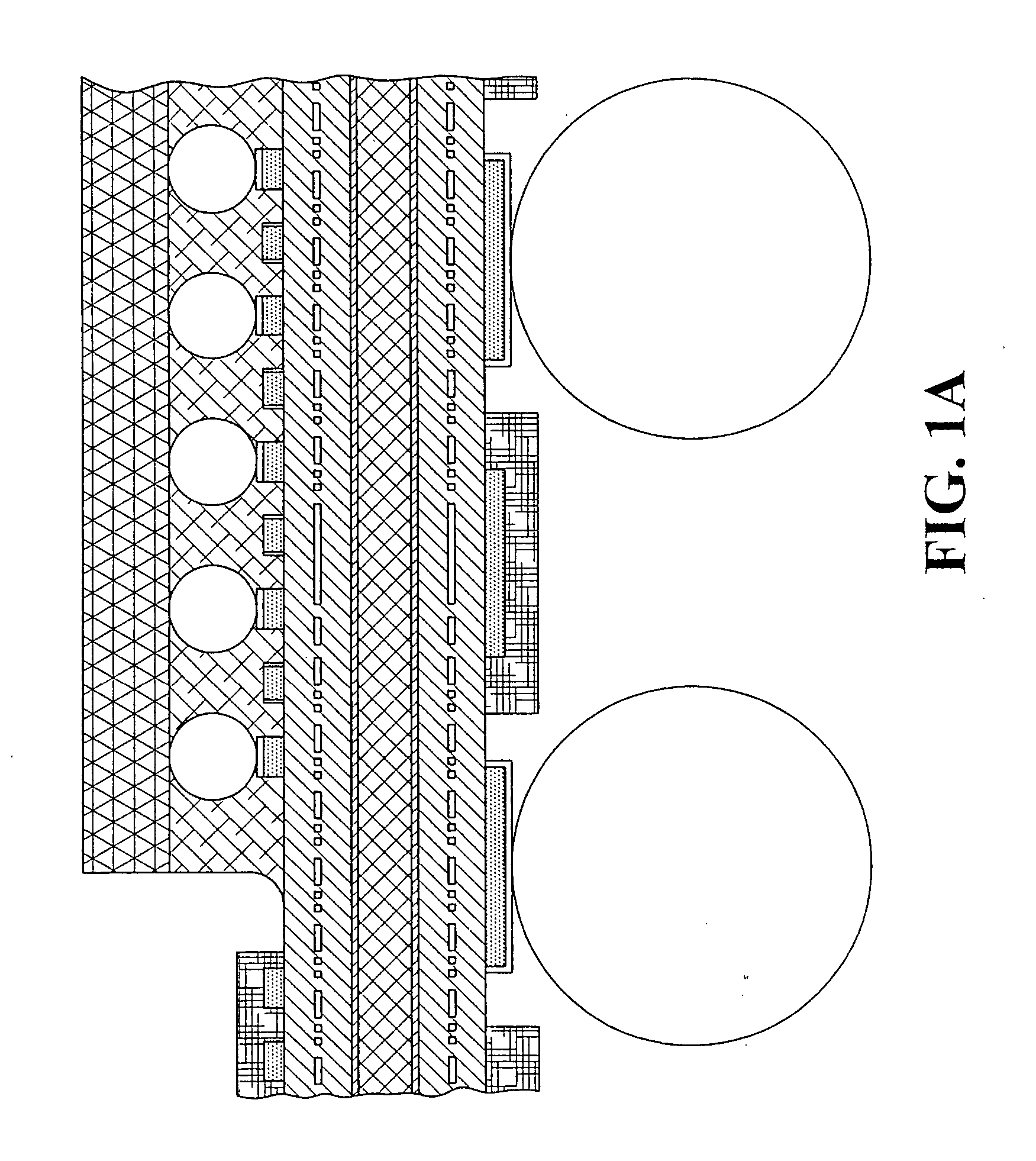
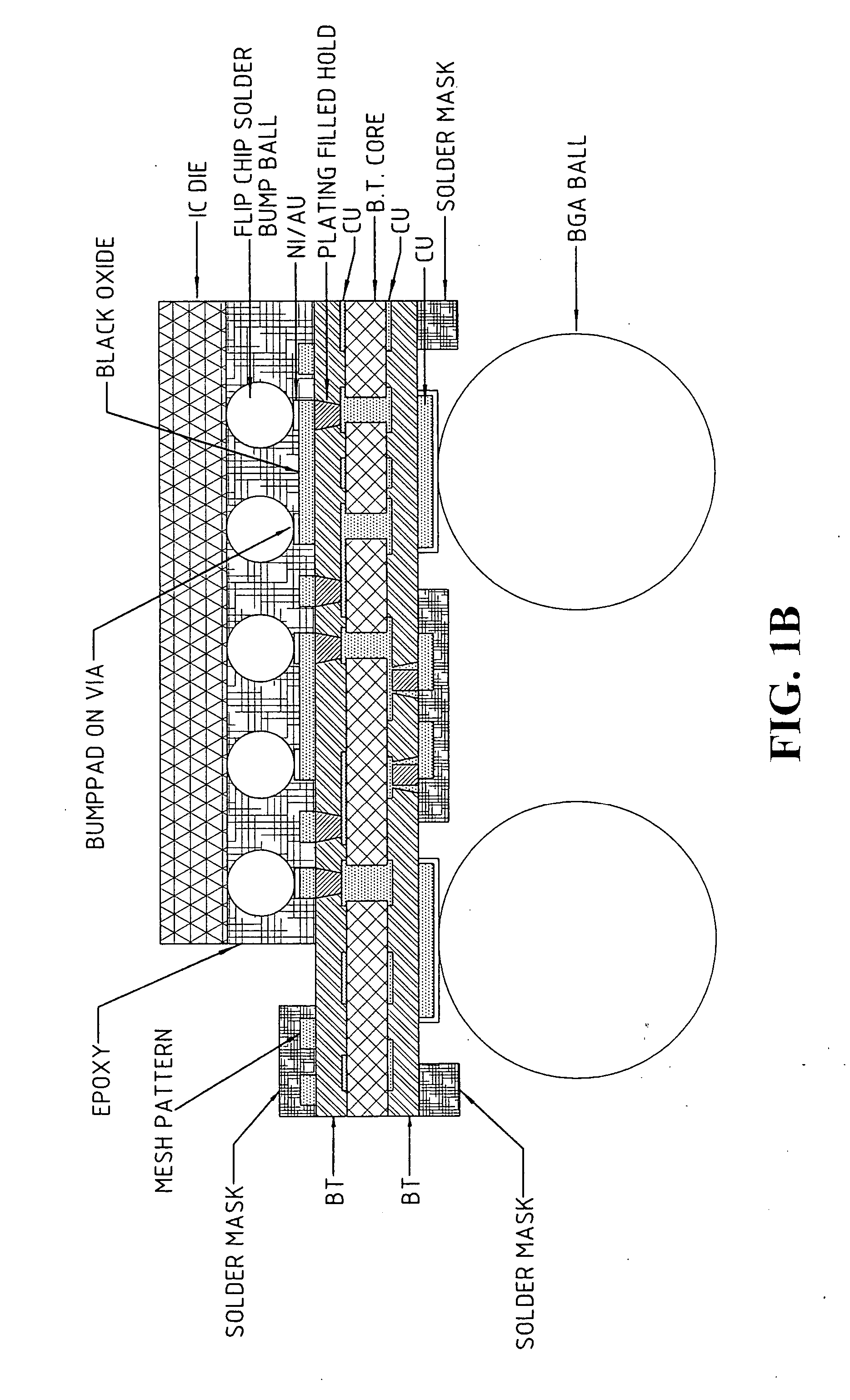
[0035]FIGS. 2A to 2C show a process of providing a substrate. FIG. 2A shows a substrate 201 which may be a flip chip substrate and is made of Bismaleimide Triazine (BT), other organic material, or even ceramics. The thickness of 201 is about 0.1 to 0.4 mm. A first metal layer 202 is made on the substrate 201. The first metal layer can be made of Copper (Cu) with a thickness of 12 μm. FIG. 2B shows a plurality of through holes 203 are drilled on the substrate 201 by mechanical or laser drilling. Each of the through holes 203 has a diameter of 100 to 250 μm. FIG. 2C shows that a first metal plated layer 204 is formed on the first metal layer 202 and the through holes 203. The first metal plated layer 204 can be made of Copper (Cu) with a thickness of 15 μm.

[0036]FIGS. 2D to 2E show a step of forming an inner circuit. FIG. 2D uses a dry film 205 containing an image to b...


PUM


Abstract

The present invention relates to a Fine Pitch flip chip substrate. A black oxide dam is made on the metal circuit between bump pads to replace the conventional solder resist so that the bump pads will not be buried in the solder resist. A small vias is dilled by laser drilling and plated filled with copper to be used as the connection between the circuits. By this way, the density and the flexibility of routing could be improved. A mesh pattern can be made in the limited space to increase the stiffness of the substrate.

Description

CROSS-REFERENCES TO RELATED APPLICATIONS [0001] This is a division of U.S. application Ser. No. 10 / 197,066, filed Jul. 17, 2002.FIELD OF THE INVENTION [0002] The invention relates to a structure and a method of manufacturing of a substrate in the semiconductor packaging process, and more particularly to fine pitch flip chip substrates that demand high packaging precision. BACKGROUND OF THE INVENTION [0003] Due to the increase of the number of I / Os in modern electronic products, the packaging technology has evolved from the early Plug-In method to the more advanced Surface Mounting Technology (SMT) in order to meet the new demands. There are two representative SMT, the Dual-In-Line Package (DIP), by Fairchild, and Flat Package (FP), by Texas Instrument Institute. Another packaging method drawing much attention is the Ball Grid Array (BGA), which uses protruding poles arranged in an array to replace the pins of conventional Pin Grid Array (PGA). PGA is a through hole packaging technol...

Claims


Application Information

Patent Timeline
IPC IPC(8): H01L21/48H01L21/56H01L21/60H01L23/31H01L23/498H05K3/34H05K3/38H05K3/46
CPCH01L21/4857H01L21/563H01L2224/32225H01L2224/16225H01L2924/014H01L2924/01076H01L2924/0105H01L2924/01033H05K2203/0315H05K2201/2081H01L23/3128H01L23/49816H01L23/49827H01L23/49894H01L24/81H01L2224/13111H01L2224/16H01L2224/73204H01L2224/81801H01L2224/83191H01L2924/01029H01L2924/01078H01L2924/01079H01L2924/01082H01L2924/14H01L2924/15311H01L2924/18301H05K3/3452H05K3/385H05K3/4602H05K2201/10674H01L2924/00H01L2924/12042
Inventor CHANG, CHIEN-WEIHUANG, SHENG-CHUAN
Owner KINSUS INTERCONNECT TECH
Why Eureka
Try Eureka