Receiver, transceiver circuit, signal transmission method, and signal transmission system

a transceiver circuit and signal transmission technology, applied in logic circuit coupling/interface arrangement, dc level restoring means or bias distortion correction, instruments, etc., can solve the problem of slow signal transmission between a main storage device such as a dram and a processor, which is becoming a bottleneck impeding computer performance improvement, etc. problem, to achieve the effect of optimizing transmission/reception parameters and enhancing receiver sensitivity

Inactive Publication Date: 2005-02-10
FUJITSU LTD
View PDF24 Cites 45 Cited by
  • Summary
  • Abstract
  • Description
  • Claims
  • Application Information

AI Technical Summary

Benefits of technology

[0010] A first object of the present invention is to provide a transceiver circuit that can evaluate and diagnose signal transmission systems, optimize transmission / reception parameters, and enhance receiver sensitivity. It is also an object of the present invention to provide a receiver that can eliminate a large common mode voltage in a circuit used for signal transmission.
[0011] A second object of the present invention is to provide a receiver capable of achieving higher-accuracy and higher-speed signal transmission by allowing a large timing margin for the operation of a decision circuit.
[0012] A third object of the present invention is to provide a signal transmission system, a signal transmission method, and a transceiver circuit that can achieve more efficient utilization of the signal transmission line and accurately perform high-speed signal transmission using fewer signal lines, and that can extend the maximum signal line length.
[0020] In addition, according to the present invention, there is provided a receiver having a plurality of signal lines and a capacitor network having capacitors connected to the signal lines and switches for controlling the connection of the capacitors, wherein the receiver includes a common mode voltage elimination circuit for eliminating a common mode voltage present on the plurality of signal lines by connecting at least one of capacitor nodes containing the component of the common mode voltage to a node held to a specific voltage value.
[0021] According to the present invention, there is provided a receiver comprising a plurality of signal lines and a capacitor network having capacitors connected to the signal lines and switches for controlling the connection of the capacitors, wherein the receiver includes a common mode voltage elimination circuit for eliminating a common mode voltage present on the plurality of signal lines by connecting at least one of capacitor nodes containing the component of the common mode voltage to a node precharged to a specific voltage value.
[0030] The compensation voltage generating circuit may be a replica driver having the same circuit configuration as that of the driver and driven by the same data as that for the driver, and may include a unit for controlling the output amplitude and transient time of the replica driver. The driver may comprise a plurality of driver units, and the replica driver may be similar in configuration to one of the driver units constituting the driver. The compensation voltage generating circuit may further include a correction circuit for generating, based on a past output bit, a correction signal for improving the accuracy of the compensation voltage at decision timing in the receiver.

Problems solved by technology

For example, the speed of signal transmission between a main storage device such as a DRAM and a processor is becoming a bottleneck impeding performance improvement for a computer as a whole.

Method used


Image

  • Receiver, transceiver circuit, signal transmission method, and signal transmission system
  • Receiver, transceiver circuit, signal transmission method, and signal transmission system
  • Receiver, transceiver circuit, signal transmission method, and signal transmission system

Examples


first embodiment

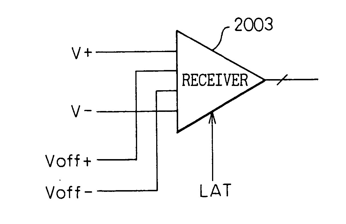
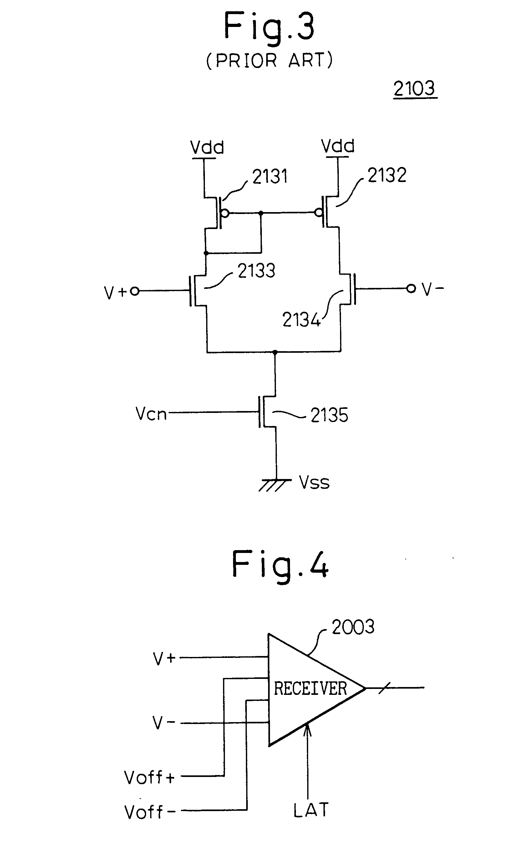
[0129]FIG. 7 is a circuit diagram showing a receiver as a first embodiment according to the first mode of the present invention; the receiver 2003 of FIG. 6 is shown here. In FIG. 7, reference numerals 2031 and 2032 are P-channel MOS transistors (PMOS transistors), 2033 to 2038 are N-channel MOS transistors (NMOS transistors), and 2039 is a decision circuit (latch circuit). Here, reference character Vcn represents a bias voltage applied to the gates of the transistors 2035 and 2038.

[0130] As shown in FIG. 7, the receiver 2003 comprises a preamplifier, which includes differential pair transistors 2033 and 2034 for application of input signals (input voltages V+ and V−) and differential pair transistors 2036 and 2037 for application of offset signals (offset voltages Voff+ and Voff), and a decision circuit (regenerative latch circuit) 2039 which makes a decision on the output of the preamplifier. More specifically, the positive logic input signal V+ is applied to the gate of one trans...

second embodiment

[0132]FIG. 8 is a block circuit diagram showing a receiver as a second embodiment according to the first mode of the present invention. In FIG. 8, reference numeral 2004 is a D / A converter for converting a digital offset code into analog form for output.

[0133] As shown in FIG. 8, the second embodiment differs from the first embodiment shown in FIG. 7 by the inclusion of a means for increasing or decreasing the offset level (offset value: offset voltage). More specifically, while applying, for example, a test pattern repeatedly in a periodic fashion, the offset value is varied in incremental steps from a minimum value toward a maximum value using the D / A converter 2005, to observe where the decision value changes from a 0 to a 1 or vice versa. With this configuration, the signal value (V+, V−) applied to the receiver (decision circuit) 2003 can be found with an accuracy equivalent to the resolution of the D / A converter 2005, and analog-like values of the received signal (the level of...

third embodiment

[0136]FIG. 10 is a block circuit diagram showing a receiver as a third embodiment according to the first mode of the present invention. In FIG. 10, reference numeral 2006 is a phase interpolator, and 2007 is a controller.

[0137] As is apparent from the comparison between FIGS. 8 and 10, the third embodiment includes, in addition to the above-described configuration of the second embodiment, a means (phase interpolator 2006) for shifting the receive timing (decision timing) relative to the received signal (input signal). Various known configurations can be employed for the phase interpolator 2006.

[0138] The receiver 2003 (the decision circuit 2039) operates, for example, at the rising edge of a timing pulse LAT supplied from the phase interpolator 2006. The phase code applied to the phase interpolator 2006 is controlled, for example, by a 6-bit digital signal from a clock recovery circuit (not shown) during usual signal reception, but is controlled by a signal supplied from a separat...


PUM


Abstract

A receiver has an offset application circuit for applying a known offset to an input signal, and a decision circuit for comparing the offset-applied input signal with a reference voltage. The level of the input signal is determined based on the known offset and on the result output from the decision circuit. With this configuration, a large common mode voltage can be eliminated in a circuit used for signal transmission.

Description

BACKGROUND OF THE INVENTION [0001] 1. Field of the Invention [0002] The present invention relates to a signal transmission technology and, more particularly, to a receiver, a transceiver circuit, a signal transmission method, and a signal transmission system for performing high-speed signal transmission between LSI chips or between a plurality of devices or circuit blocks accommodated on the same chip, or between boards or enclosures. [0003] 2. Description of the Related Art [0004] In recent years, the performance of components used to construct computers and other information processing apparatuses has improved greatly; for example, performance improvements for semiconductor memory devices such as DRAM (Dynamic Random Access Memory) and processors and the like have been remarkable. The improvements in the performance of semiconductor memory devices, processors, etc. have come to the point where system performance cannot be improved further unless the speed of signal transmission be...

Claims


Application Information

Patent Timeline
Patent Type & Authority Applications(United States)
IPC IPC(8): G06F3/00G06F13/00H03F3/45H03K19/0175H04L5/14H04L7/02H04L7/033H04L7/04H04L25/02H04L25/06H04L25/08
CPCH03F3/45183H03F3/45475H03F3/45762H03F3/45986H04L25/061H04L5/1461H04L7/033H04L25/0274H04L25/0292H04L5/14G06F13/00
Inventor TAMURA, HIROTAKA
Owner FUJITSU LTD
Why Eureka
Try Eureka