Beam irradiation apparatus, beam irradiation method, and method for manufacturing a thin film transistor

Inactive Publication Date: 2005-02-17
SEMICON ENERGY LAB CO LTD
View PDF20 Cites 79 Cited by
  • Summary
  • Abstract
  • Description
  • Claims
  • Application Information

AI Technical Summary

Benefits of technology

[0029] Uniform laser irradiation can be performed to the irradiated object according to the present invention. When the semiconductor film is used as the irradiated object, the poly-crystalline TFT having uniform crystallinity and uniform electric characteristic can be formed. Moreover, since the beam spot can be scanned at a constant speed on the irradiated object and since the scanning position of the spot can be contr

Problems solved by technology

However, the use of the above scanning means might cause a problem that the scanning speed and the irradiated state are not uniform in the end portions of the irradiated surface where the scanning starts and the scanning ends.
In addition, the vibration of the galvanometer mirror might make the scanning width meander.
Although the galvanometer mirror can increase or decrease the scanning speed in a short time, the present inventor recognized that such inhomogeneous laser irradiat

Method used


Image

  • Beam irradiation apparatus, beam irradiation method, and method for manufacturing a thin film transistor
  • Beam irradiation apparatus, beam irradiation method, and method for manufacturing a thin film transistor
  • Beam irradiation apparatus, beam irradiation method, and method for manufacturing a thin film transistor

Examples


embodiment

[0040] Embodiment Mode 1

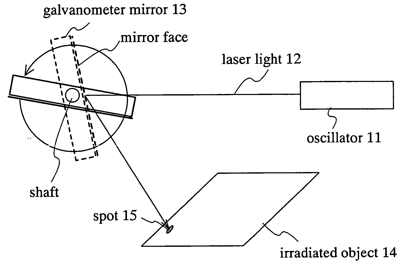
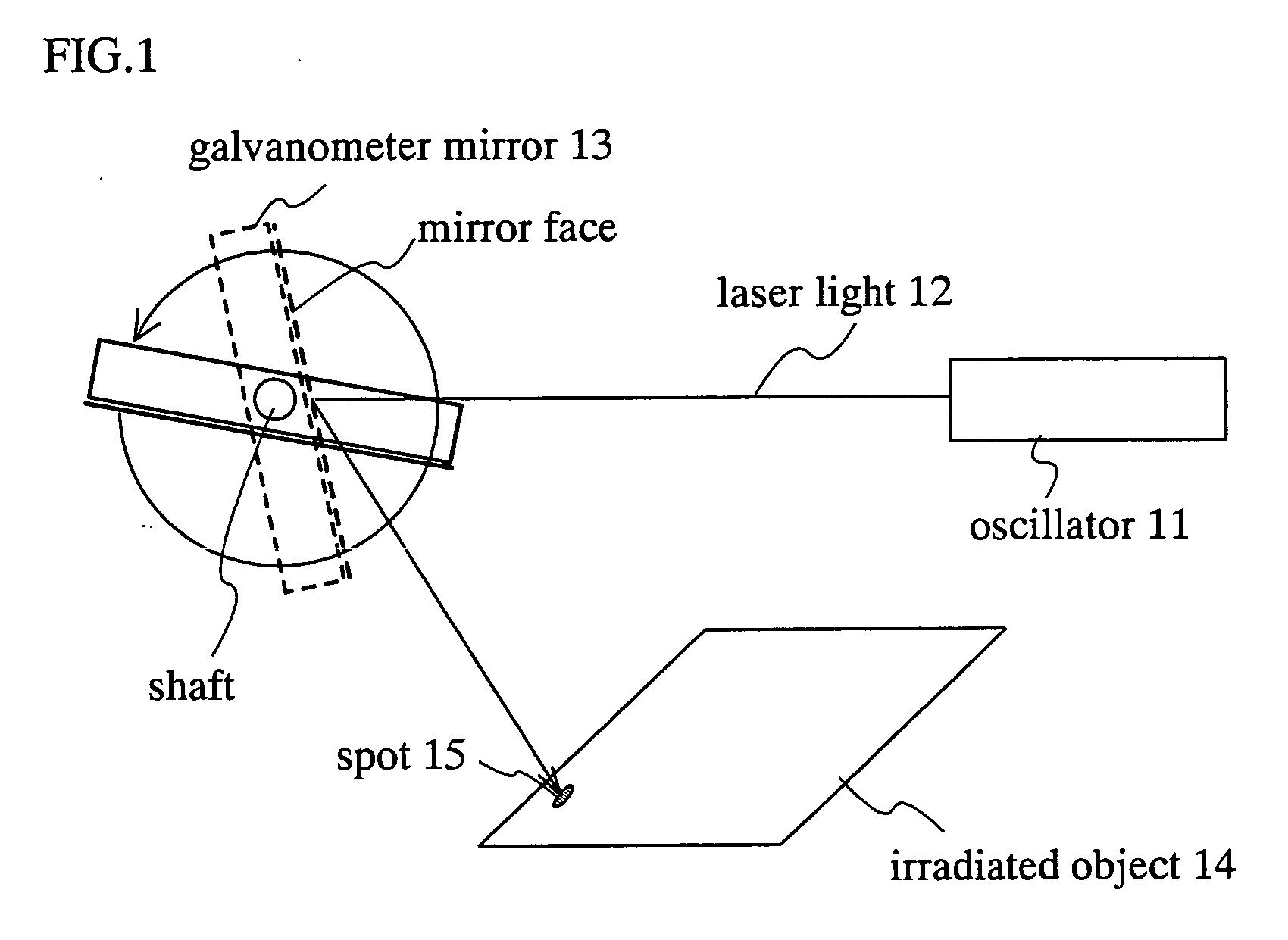
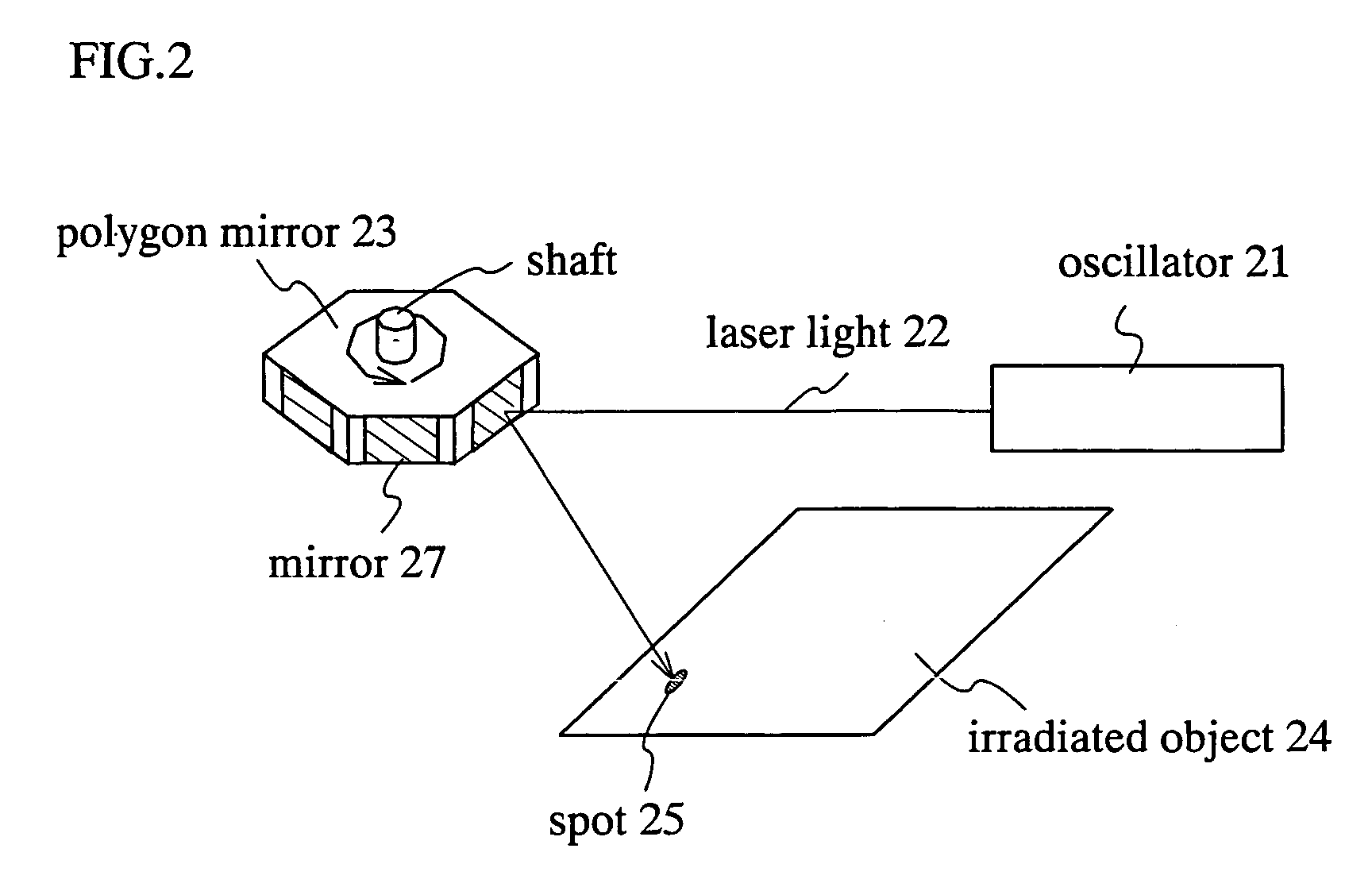
[0041] The present embodiment mode explains the case where a rotating galvanometer mirror is used as the scanning means and a semiconductor film is used as the irradiated object and where a poly-crystalline TFT is formed by crystallizing the semiconductor film.

[0042]FIG. 3 shows a laser irradiation apparatus including an oscillator 101 for emitting a CW laser (also referred to as a continuous wave laser), an optical system 102 for shaping a laser beam emitted from the oscillator into linear, a galvanometer mirror for scanning the linear laser beam on a semiconductor film, a shaft 108 for rotating the galvanometer mirror, a control apparatus 110 for controlling the shaft and the rotation of the galvanometer mirror, and an fθ lens 104 for making the shape of the laser beam on the irradiated surface constant. The laser beam emitted from the oscillator is incident into the optical system so that its shape becomes linear laser beam (hereinafter this beam is refer...


PUM

PropertyMeasurementUnit
Energyaaaaaaaaaa
Semiconductor propertiesaaaaaaaaaa

Abstract

A galvanometer mirror rotates in one direction when the galvanometer mirror is used. A spot can be scanned on an irradiated surface at a more constant speed by rotating the galvanometer mirror and by using the inertia. Moreover, it is preferable to make the galvanometer mirror heavy because the inertia becomes higher so that the spot is scanned at a more constant speed. In addition, in a polygon mirror of this invention, mirrors are arranged so as not to contact each other because a change time of the scanning position between the mirrors is provided. By moving the irradiated object with timing together when the laser light is not irradiated, the laser process can be performed efficiently.

Description

BACKGROUND OF THE INVENTION [0001] 1. Field of the Invention [0002] The present invention relates to a beam irradiation apparatus and a beam irradiation method. Moreover, the present invention relates to a method for manufacturing a thin film transistor using the apparatus and the method. [0003] 2. Description of Related Art [0004] In recent years, a research has been conducted concerning a thin film transistor having a channel-forming region in a poly-crystalline semiconductor film (hereinafter this thin film transistor is referred to as a poly-crystalline TFT) as a semiconductor element in a display device, an integrated circuit, or the like. With the development of the display device and the integrated circuit, further enhancement of the characteristic of the poly-crystalline TFT has been demanded. [0005] Consequently, as one means to obtain the poly-crystalline TFT, a laser irradiation apparatus including a continuous wave laser and means for scanning a laser beam (also referred...

Claims


Application Information

Patent Timeline
IPC IPC(8): G02B26/10
CPCG02B26/105Y10S359/90
Inventor TANAKA, KOICHIRO
Owner SEMICON ENERGY LAB CO LTD
Why Eureka
Try Eureka