Pattern production system, exposure system, and exposure method

a technology of exposure system and pattern, applied in the field of pattern production system, can solve the problems of over-etching, copper eroded by etching, and repeated use of etching liquid, and achieve the effect of high finish and without adding to cos

Inactive Publication Date: 2005-02-17
FUJIFILM CORP +1
View PDF0 Cites 15 Cited by
  • Summary
  • Abstract
  • Description
  • Claims
  • Application Information

AI Technical Summary

Benefits of technology

In view of the foregoing observations and description, the primary object of the present invention is to provide a pattern production system which can produce a pattern at high finish without affected by deterioration of the developer and the etching liquid or the like and without adding to the cost.
If the resist is exposed to light through a mask pattern depicted on a film or glass substrate as in a conventional method, it is necessary to often remake the mask pattern to deal with such fluctuation, which adds to the cost. However, by exposing the resist to light, by direct drawing by the use of a direct drawing exposure system, at the adjusted exposure and / or with the adjusted line width, uniform finish can be obtained without adding to the cost.
Further, if the relation between the value of correction, by which the width of the line forming the pattern is corrected and the result of comparison is stored for each of the regions formed by dividing the circuit board into a plurality of regions, the correction can be made to nullify the localism inherent to the production system, which results in more precise and more uniform finish.

Problems solved by technology

In the conventional technology, there has been a problem that the amount of copper eroded by etching fluctuates depending on the line density of the resist pattern, which in turn fluctuates the width of the line forming the finished circuit pattern.
Further, when the width of the line forming the resist pattern is not larger than a predetermined width, over-etching occurs.
Further, the etching liquid can deteriorate after repeated use and the width of the line forming the etched circuit pattern can fluctuate.
According to the methods disclosed in Japanese Unexamined Patent Publication Nos. 6(1994)-186724 and 2001-134627, though the width of the line forming the etched circuit pattern approximates a designated line width by correcting the line width represented by input data, the fluctuation in finish due to deterioration of developer or etching liquid after repeated use thereof cannot be suppressed.
Further, the photo-mask must be remade a plurality of times in order to suppress the fluctuation in finish, for instance, due to deterioration of the etching liquid and the production cost rises.
However, the method is disadvantageous in that due to instable response, control of supply of new etching liquid and / or the shower pressure of the etching liquid cannot fully remove the fluctuation in finish.
With increasing complication and / or increasing fineness of the circuit pattern, more precise finish recently has come to be desired and the fluctuation in finish, for instance, due to deterioration of the etching liquid has become unignorable.

Method used


Image

  • Pattern production system, exposure system, and exposure method
  • Pattern production system, exposure system, and exposure method
  • Pattern production system, exposure system, and exposure method

Examples


first embodiment

A pattern production system in accordance with the present invention will be described with reference to the drawings.

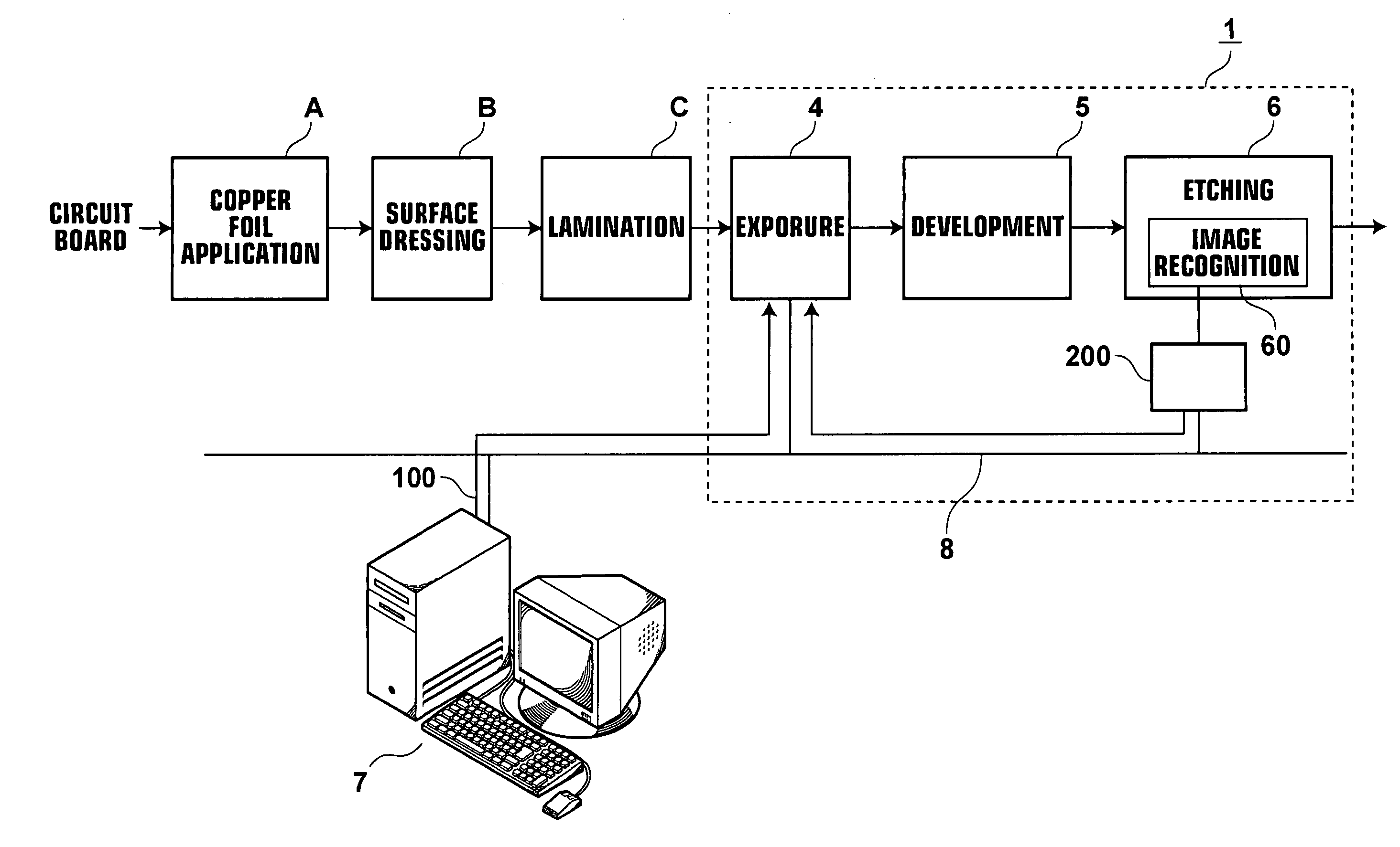
FIG. 1 is a block diagram showing a pattern production system 1 in accordance with a first embodiment of the present invention. Production of a circuit pattern (an etched pattern) by the pattern production system 1 will be described, hereinbelow. First, copper foil, which is a circuit formation material, is applied to a circuit board in copper foil applying step A. The upper surface of the copper foil is dressed by mechanical polishing, chemical polishing or the like in surface dressing step B. Then resist (resist material) is laminated on the dressed upper surface of the copper foil in lamination step C. Thereafter, by the pattern production system 1 in accordance with the first embodiment of the present invention, a desired etched pattern is formed by exposing to light the resist on the circuit board, developing the exposed resist to form a resist pattern and etchi...

third embodiment

A pattern production system in accordance with the present invention will be described, hereinbelow.

FIG. 12 is a block diagram showing a pattern production system 11 in accordance with the third embodiment of the present invention. Production of a circuit pattern (an etched pattern) by the pattern production system 11 will be described, hereinbelow. First, copper foil which is a circuit formation material is applied to a substrate in copper foil applying step A. The upper surface of the copper foil is dressed by mechanical polishing, chemical polishing or the like in surface dressing step B. Then resist (resist material) is laminated on the dressed upper surface of the copper foil in lamination step C. Thereafter, by the pattern production system 11 according to the present invention, a desired etched pattern is formed by exposing to light the resist on the circuit board, developing the exposed resist to form a resist pattern and etching the copper foil on the substrate, on which th...


PUM

PropertyMeasurementUnit
shapeaaaaaaaaaa
widthaaaaaaaaaa
areaaaaaaaaaaa

Abstract

In a pattern production system, resist coated on copper foil on the substrate is exposed to light, by direct drawing, on the basis of a width of a line forming a pattern designated by processing pattern data at a predetermined exposure, the exposed resist is developed to form a resist pattern, and the copper foil is etched to form an etched pattern. An image of the etched pattern is scanned and image information of the etched pattern is obtained. The width of the line forming the pattern represented by the image information and the width of the line forming the pattern of the target etched pattern are compared, and the width of the line forming the pattern designated by the processing pattern data is adjusted on the basis of the result of comparison. The resist is exposed to light, by direct drawing, with the adjusted line width on the basis of the result of comparison.

Description

BACKGROUND OF THE INVENTION 1. Field of the Invention This invention relates to a pattern production system in which fluctuation in finish, for instance, in a circuit pattern of a printed circuit board due to deterioration of developer and / or etching liquid can be suppressed. 2. Description of the Related Art For example, when producing a circuit pattern of a printed circuit board, in the past, a resist layer on a circuit board had been selectively exposed to light and solidified by the use of a photo-mask, the resist layer had been developed to form a resist pattern and the circuit pattern had been formed by etching copper foil on the substrate by the use of the resist pattern. In the conventional technology, there has been a problem that the amount of copper eroded by etching fluctuates depending on the line density of the resist pattern, which in turn fluctuates the width of the line forming the finished circuit pattern. In order to overcome this problem, there has been propo...

Claims


Application Information

Patent Timeline
Patent Type & Authority Applications(United States)
IPC IPC(8): G03D5/00G03F1/00G03F7/20G03F7/26H05K1/02H05K3/00H05K3/06
CPCG03F7/2053H05K1/0269H05K2203/163H05K3/064H05K2203/107H05K3/0082G03F7/20
Inventor MORITA, SEIKINAKAYA, DAISUKESAWANO, MITSURUSUGANUMA, ATSUSHI
Owner FUJIFILM CORP
Why Eureka
Try Eureka