Method of forming metal interconnection layer of semiconductor device

a metal interconnection layer and semiconductor technology, applied in semiconductor/solid-state device manufacturing, basic electric elements, electric devices, etc., can solve the problems of increasing the total power consumption of a semiconductor chip, increasing the amount of signal leakage from the semiconductor chip, and deteriorating the electrical performance of a semiconductor device, so as to eliminate problems and disadvantages

Inactive Publication Date: 2005-02-17
SAMSUNG ELECTRONICS CO LTD
View PDF12 Cites 62 Cited by
  • Summary
  • Abstract
  • Description
  • Claims
  • Application Information

AI Technical Summary

Benefits of technology

[0016] Exemplary embodiments of the invention generally include improved methods for forming a metal interconnection layer of a semiconductor device, which are capable of eliminating problems and disadvantages associated with conventional methods such as described above.

Problems solved by technology

Indeed, parasitic resistance and capacitance components in a metal interconnection framework may cause, e.g., signal delay, which can deteriorate the electrical performance of a semiconductor device.
In addition, parasitic resistance and capacitance components can increase the total power consumption of a semiconductor chip and increase the amount of signal leakage from the semiconductor chip.
However, it has proven difficult to form a Cu interconnection layer using a typical photolithography-based patterning process.
There are various disadvantages associated with the conventional method depicted in FIGS. 1-3.
Furthermore, when the sacrificial layer 116 is formed of an inorganic material, such as hydrogen silsesquioxane (HSQ), there is a need to further perform a stripping process to remove the sacrificial layer 116, which is a very complicated and difficult process.

Method used


Image

  • Method of forming metal interconnection layer of semiconductor device
  • Method of forming metal interconnection layer of semiconductor device
  • Method of forming metal interconnection layer of semiconductor device

Examples


Embodiment Construction

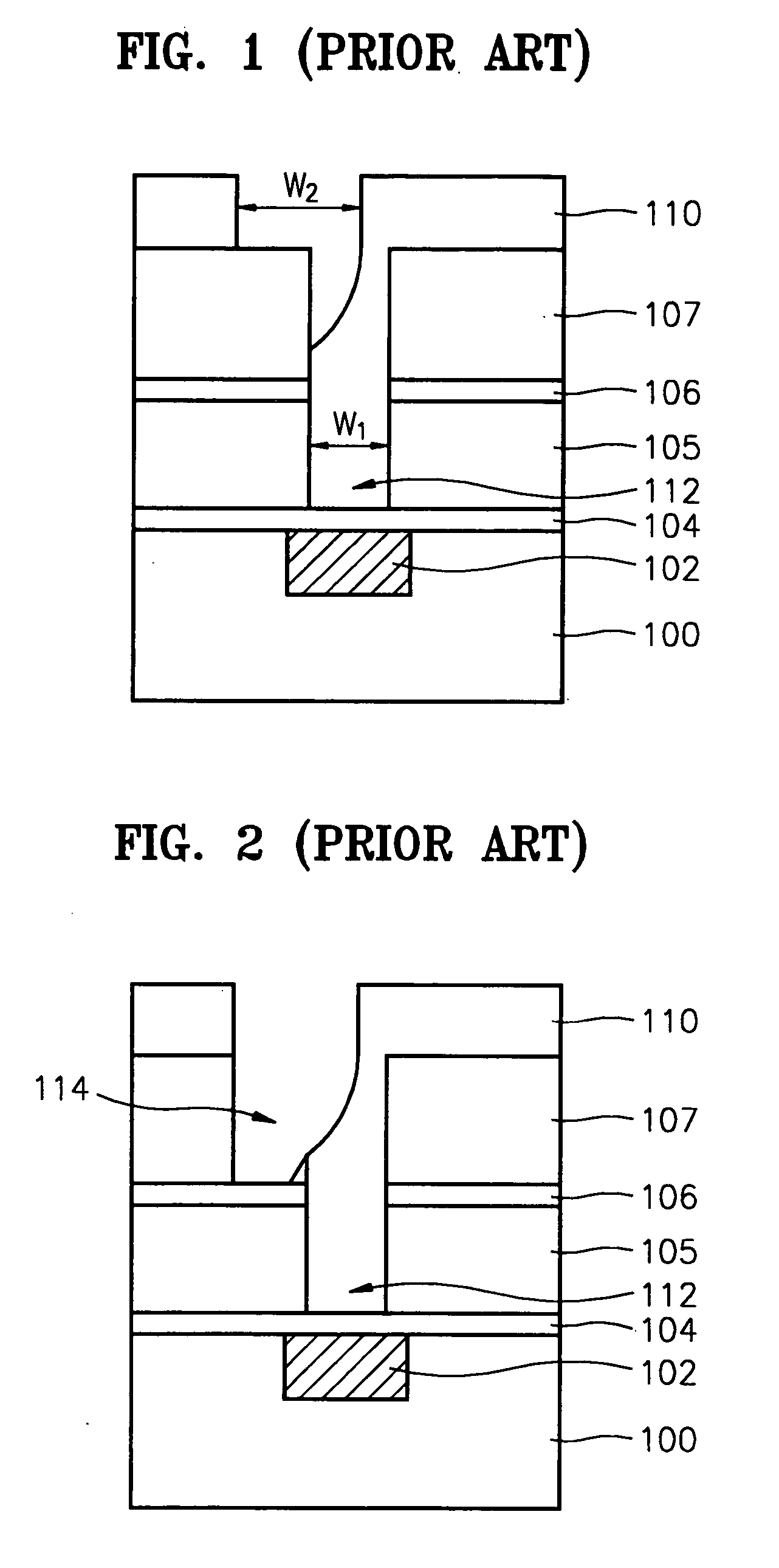
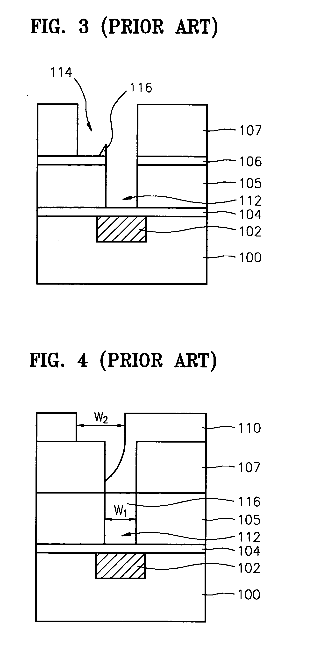
[0025] Hereinafter, exemplary embodiments of the present invention will be described more fully with reference to the accompanying drawings. These exemplary embodiments are provided so that this disclosure will be thorough and complete, and will fully convey concepts of the invention to one of ordinary skill in the art. However, one of ordinary skill in the art could readily envision other embodiments of the invention and nothing herein should be construed as limiting the scope of the invention. Further, it is to be understood that the drawings are schematic representations where the thickness of layers and regions are exaggerated for clarity. Moreover, the same reference numerals throughout the drawings may represent the same or similar elements, and thus their description may be omitted.

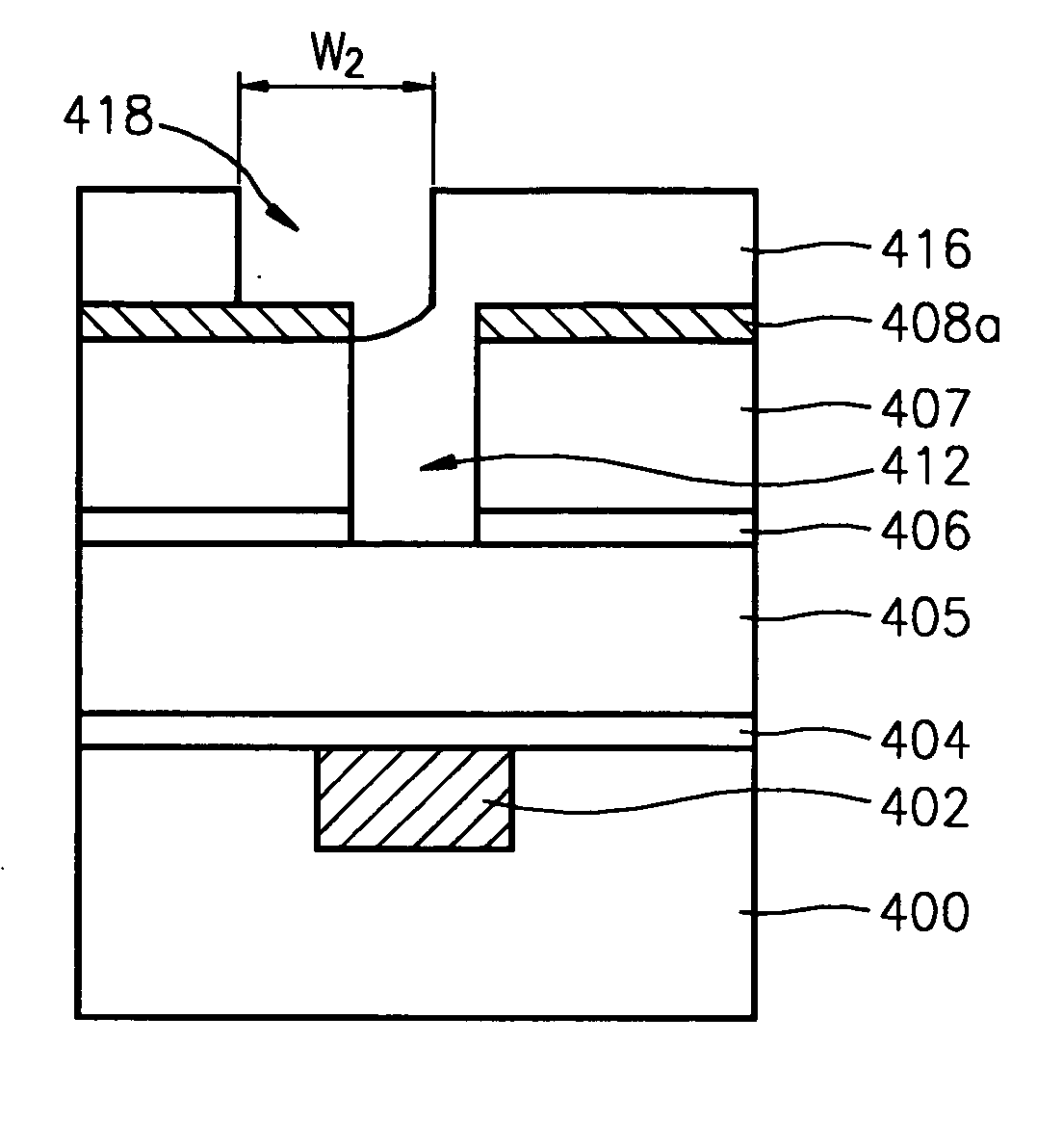
[0026]FIGS. 7 through 14 are cross-sectional schematic views illustrating a method for forming a metal interconnection layer of a semiconductor device according to an exemplary embodiment of the p...


PUM

PropertyMeasurementUnit
areaaaaaaaaaaa
thicknessaaaaaaaaaa
depthaaaaaaaaaa

Abstract

Various methods are provided for forming metal interconnection layers of semiconductor devices. One exemplary method for forming a metal interconnection layer of a semiconductor device includes forming an interlayer dielectric layer on a substrate, forming a hard mask layer on the interlayer dielectric layer, wherein the hard mask layer serves as an anti-reflection layer, depositing and patterning a first photoresist layer to form a first photoresist pattern on the hard mask layer, forming a partial via hole in the interlayer dielectric layer by etching the hard mask layer and the interlayer dielectric layer using the first photoresist pattern as an etching mask, removing the first photoresist pattern, depositing a second photoresist layer to fill the partial via hole with photoresist material and patterning the second photoresist layer to form a second photoresist pattern that defines a trench interconnection area which overlaps at least portion of the partial via hole, etching the hard mask layer using the second photoresist pattern as an etching mask to form a hard mask pattern, completely removing the second photoresist pattern and the photoresist material in the partial via hole, etching the interlayer dielectric layer using the hard mask pattern as an etching mask to form the trench interconnection area and to extend the partial via hole to form a full via hole, and filling the full via hole and the trench interconnection area with a conductive material.

Description

CROSS-REFERENCE TO RELATED APPLICATIONS [0001] This application is a Continuation-in-Part of U.S. patent application Ser. No. 10 / 392,710, filed on Mar. 20, 2003, which claims priority to Korean Patent Application No. 02-27442, filed on May 17, 2002, and which is Continuation-in-Part of U.S. patent application Ser. No. 10 / 114,274, filed on Apr. 2, 2002, which claims priority to Korean Patent Application No. 01-26966 filed on May 17, 2001, all of which are fully incorporated herein by reference. [0002] In addition, this application claims priority to Korean Patent Application No. 03-47006, filed on Jul. 10, 2003, which is fully incorporated herein by reference.TECHNICAL FIELD OF THE INVENTION [0003] The present invention relates to methods for manufacturing semiconductor devices, and more particularly, to improved methods for forming metal interconnection layers of semiconductor devices using a dual damascene process. BACKGROUND [0004] Due to the continuing increase in integration den...

Claims


Application Information

Patent Timeline
Patent Type & Authority Applications(United States)
IPC IPC(8): H01L21/768
CPCH01L21/76813H01L21/76808
Inventor KIM, IL-GOOHAH, SANG-ROKSON, SAE-ILLEE, KYOUNG-WOO
Owner SAMSUNG ELECTRONICS CO LTD
Why Eureka
Try Eureka