Pixel element substrate, display device, electronic device, and method for manufacturing the pixel element substrate

a technology of electronic devices and substrates, applied in the field of display devices, can solve the problems of reducing significantly affecting the image quality, and difficult to apply uniform voltage to the organic el elements constituting the screen, so as to improve the aperture efficiency of the display region, and reduce the resistance of electronic materials.

Inactive Publication Date: 2005-02-24
SEIKO EPSON CORP
View PDF5 Cites 32 Cited by
  • Summary
  • Abstract
  • Description
  • Claims
  • Application Information

AI Technical Summary

Benefits of technology

[0024] According to the present invention, since pixel electrodes having a small area are arranged on the transparent (transmissive) substrate side, a high conductive metal having Al, Cu, or Cr is used for a common electrode on the side of the pixel element substrate facing the driving circuit. Thus, even though an electrode material having a high resistance value, for example, ITO is used on the transparent (transmissive) substrate side, the nonuniformity of brightness of an image due to a voltage drop hardly occurs. Further, since auxiliary wiring of a mesh form is not required at the peripheries of pixels in order to reduce the resistance of an electronic material having a high resistance, the aperture efficiency of a display region can be improved.

Problems solved by technology

When it has a large screen (large area), it becomes difficult to apply uniform voltage to the organic EL elements constituting the screen due to the voltage drop.
When it is impossible to apply uniform driving voltage to the organic EL elements, non-uniform light emission occurs, which significantly affects the image quality.
However, when the width of the auxiliary wiring is widened to lower the resistance value, a light emitting region becomes smaller and the aperture efficiency is reduced.
Accordingly, it becomes difficult that a common electrode is set to a sufficiently low resistance value.

Method used


Image

  • Pixel element substrate, display device, electronic device, and method for manufacturing the pixel element substrate
  • Pixel element substrate, display device, electronic device, and method for manufacturing the pixel element substrate
  • Pixel element substrate, display device, electronic device, and method for manufacturing the pixel element substrate

Examples


embodiment 1

[0041] [Embodiment 1]

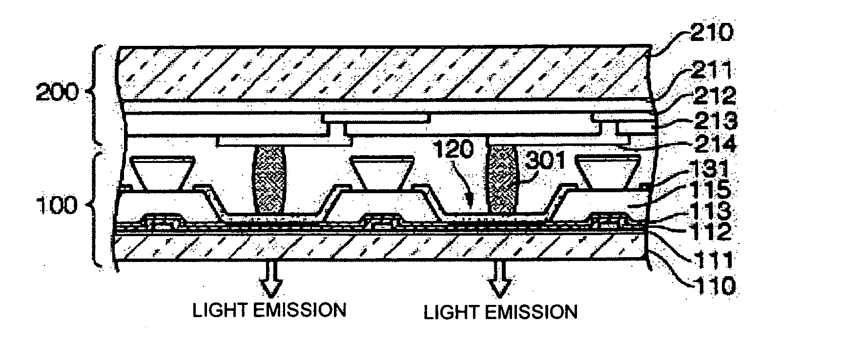
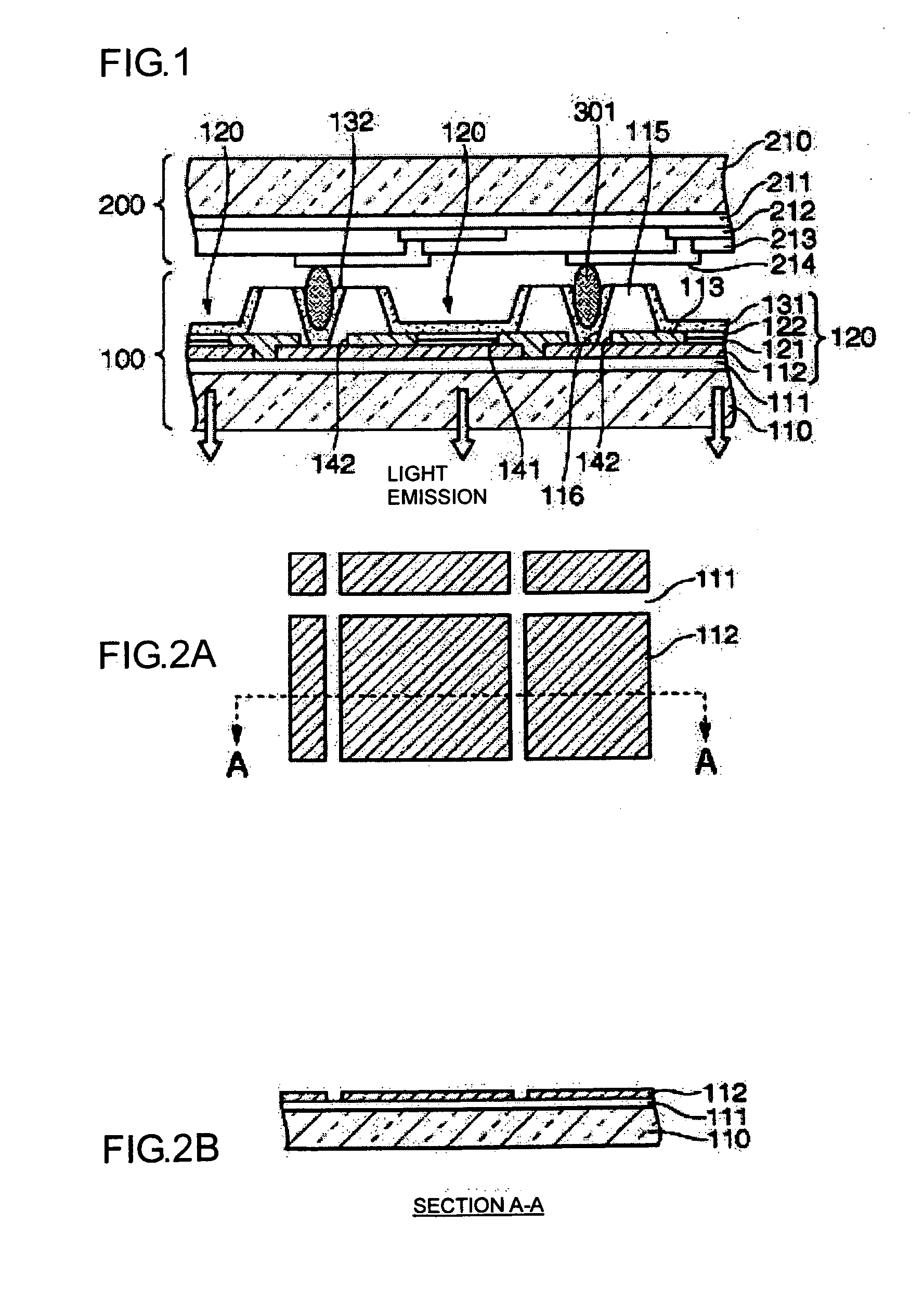
[0042]FIG. 1 shows a display device according to an embodiment of the present invention. The display device is roughly classified into a pixel element substrate 100 and a driving circuit substrate 200.

[0043] First, the pixel element substrate 100 includes a substrate 110, an insulating layer 111, a transparent pixel electrode 112, an insulating layer 113, a bank layer 115, a through-hole 116, an organic EL element 120 as a pixel element, and a common electrode layer 131.

[0044] The substrate 110 is a transparent substrate that is made of non-alkaline glass, such as quartz glass, or plastic film. As described below, the insulating layer 111 is formed on the substrate 110. A plurality of the pixel electrodes 112 is patterned in a quadrangular form and arranged on the insulating layer 111. The pixel electrodes 112 are made of transparent ITO. The periphery and the upper surface of the pixel electrode 112 are coated with an insulating layer 113, and are isolated (i...

embodiment 2

[0058] [Embodiment 2]

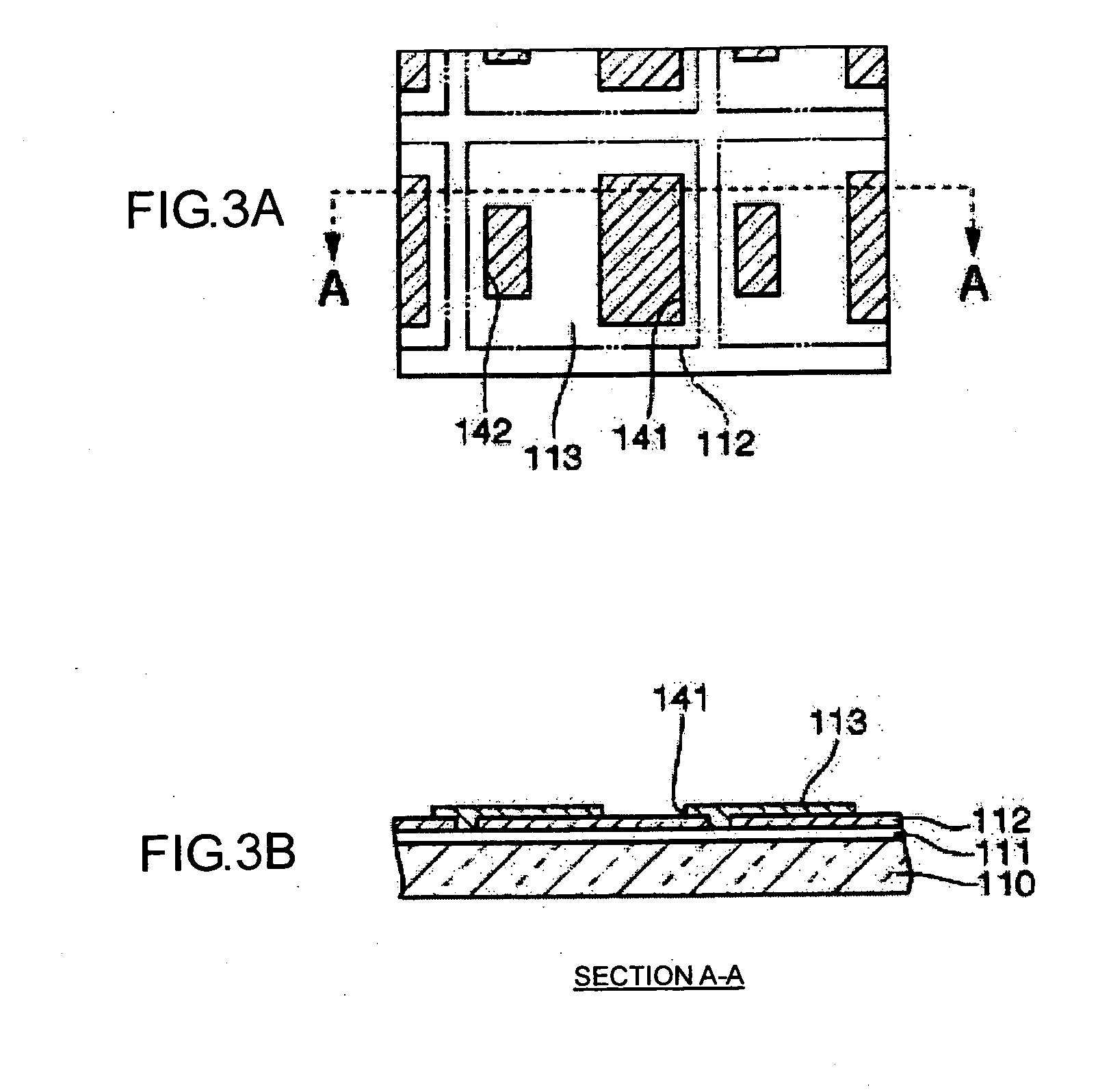
[0059] Hereinafter, a process for manufacturing a pixel element substrate of a display device according to the present invention will be described with reference to FIGS. 2 to 9. Each (a) of FIGS. 2 to 8 is a plan view of the pixel element substrate. Each (b) of FIGS. 2 to 8 is a sectional view taken along the line A-A in FIGS. 2(a) to 8(a). Each (c) of FIGS. 5 to 8 is a sectional view taken along the line B-B in the plan view.

[0060] First, as shown in FIG. 2, on a non-alkaline glass substrate 110 having a thickness of 0.5 mm, for example, TEOS is dissolved in a film forming device by a plasma CVD method to form silicon oxide film of about 5000 Å, so that an insulating film 111 is formed. On the resulting object, an ITO film of about 500 Å is applied to form a transparent electrode layer. Then, using a mask (not shown) of a pixel electrode, a transparent electrode layer is patterned to form a plurality of pixel electrodes 112.

[0061] As shown FIG. 3, a silicon ...

embodiment 3

[0070] [Embodiment 3]

[0071] Hereinafter, several examples of an electronic apparatus including the above-described display device (organic EL display device) will be explained.

[0072]

[0073] First, an example in which the organic EL display device 1 according to the embodiment is used for a mobile personal computer having will be described. FIG. 12 is a perspective view showing the configuration of the mobile personal computer. In FIG. 12, the personal computer 1100 includes a main body 1104 having a keyboard 1102, and an organic EL display device 1.

[0074]

[0075] Next, an example in which the organic EL display panel is applied to a display unit of a portable telephone will be explained. FIG. 13 is a perspective view showing the configuration of the portable telephone. In FIG. 13, portable telephone 1200 includes a plurality of operating buttons 1202, an earpiece 1204, a mouthpiece 1206, and the above-described organic EL display device 1.

[0076]

[0077] Further, the example of a digit...


PUM

PropertyMeasurementUnit
thicknessaaaaaaaaaa
thicknessaaaaaaaaaa
heightaaaaaaaaaa

Abstract

To provide a display device that applies a uniform driving voltage to each pixel and prevents light emitting regions from being narrower. In a display device obtained by bonding a pixel element substrate to a driving circuit board having a driving circuit for the plurality of pixel elements, the driving circuit board includes connecting terminals connected to the driving circuit for the plurality of pixel elements on the surface of the driving circuit board facing the pixel element substrate. The pixel element substrate comprises pixel electrodes 112 formed on a transmissive substrate 110, pixel elements 120 formed on the plurality of pixel electrodes such that respective ends of the pixel elements are adjacent to each other, common electrode wiring lines 131 for commonly connecting the other respective ends of the plurality of pixel elements to each other, bank regions 115 for separating the pixel elements from each other to define individual pixel element regions, and individual electrode wiring lines 132 for connecting the connecting terminals of the driving circuit board to the corresponding pixel electrodes of the pixel elements via through-holes formed in the bank regions.

Description

BACKGROUND OF THE INVENTION [0001] 1. Field of Invention [0002] The present invention relates to a display device and a manufacturing method thereof using an electroluminescent (EL) element or a liquid crystal display element, and more specifically, it relates to a display device and a method for manufacturing the same that improves the aperture efficiency of pixels. [0003] 2. Description of Related Art [0004] The applicant filed a patent application for “An organic EL display device and a manufacturing method thereof” on Dec. 18, 2002. The patent application proposes manufacturing a display device in which an EL substrate having an organic EL element incorporated therein is bonded to a driving circuit board having a driving circuit for driving the organic EL element incorporated therein. Accordingly, for example, it allows a display device to be efficiently produced. [0005] In the proposed display device, an EL substrate having a plurality of organic EL elements arranged therein is...

Claims


Application Information

Patent Timeline
Patent Type & Authority Applications(United States)
IPC IPC(8): G02F1/01G02F1/1345G02F1/1343G09F9/00H01L21/00H01L27/32H01L51/50H05B33/00H05B33/02H05B33/10H05B33/12H05B33/14H05B33/22
CPCG02F1/1345H01L27/3253H01L27/3246H10K59/1275H10K59/122H05B33/00H05B33/10
Inventor SAKURAI, KAZUNORI
Owner SEIKO EPSON CORP
Why Eureka
Try Eureka